 Hotline: +84 - 911522133

| STT |
|---|

MicroZed™ is a low-cost SOM that is based on the AMD Xilinx Zynq®-7000 SoC. In addition to the Zynq-7000 SoC, the module contains the common functions and interfaces required to support the core of most SoC designs, including memory, configuration, Ethernet, USB, and clocks. On the bottom side of the module, MicroZed contains two 100-pin I/O headers that provide connection to two I/O banks on the programmable logic (PL) side of the Zynq-7000 SoC device. When plugged onto a user designed baseboard or carrier card, these 100-pin connectors provide connectivity between the Zynq-7000 SoC PL I/Os and the user circuits on the carrier card. MicroZed also includes on-board power regulation that supports 5 V input with an option to support 12 V input.
Industrial Temperature MicroZed SOMs are built with components supporting extended temperatures of -40 to +85°C, with the exception of the use of the microSD card connector. Due to the configurability of the Zynq device, the user must perform final temperature testing validation.
Key Features
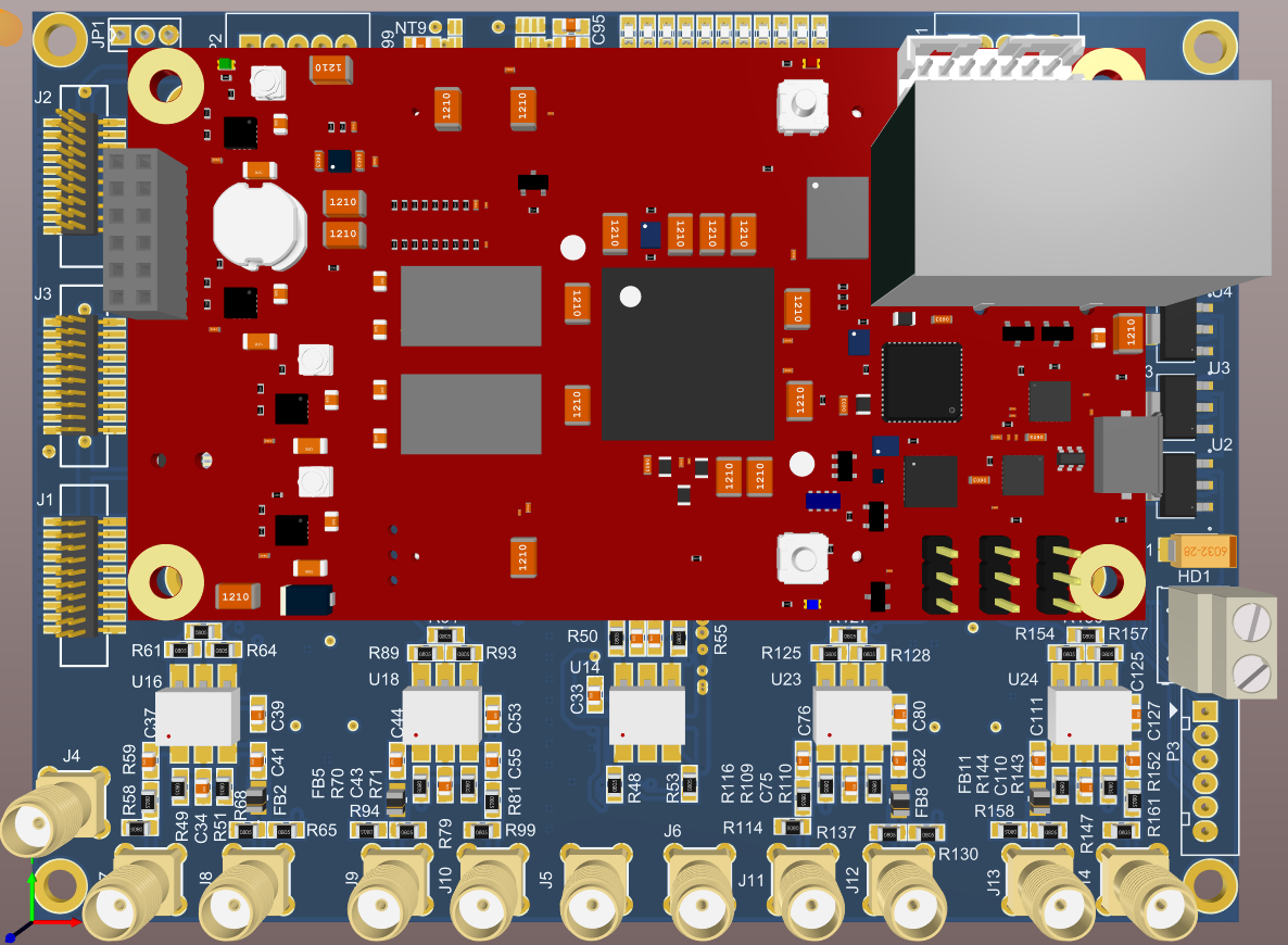
Here is 3D image of PCB on 100MSPS High Speed ADC - 4 Channel
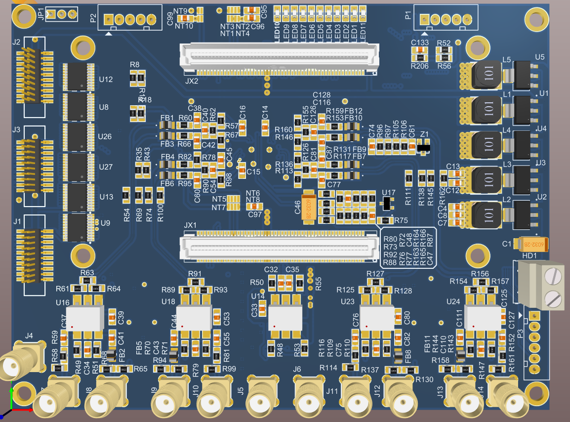
Here is 3D TOP image of PCB on 100MSPS High Speed ADC - 4 Channel
Here is 3D Bottom image of PCB on 100MSPS High Speed ADC - 4 Channel

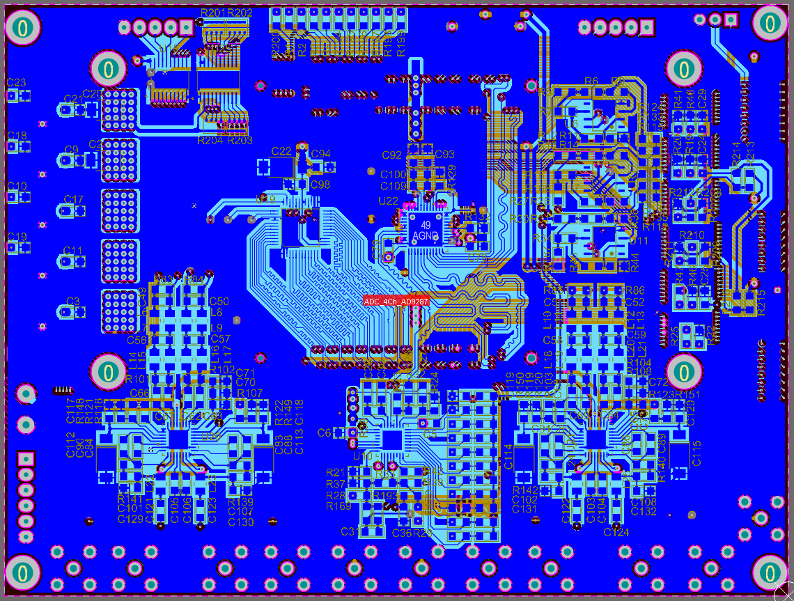
Here is 2D Top layer image on PCB of 100MSPS High Speed ADC - 4 Channel

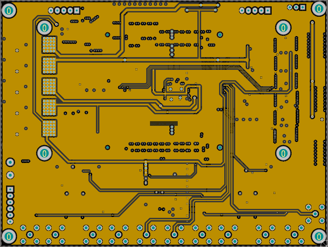
Here is 2D layer1 image of PCB on 100MSPS High Speed ADC - 4 Channel
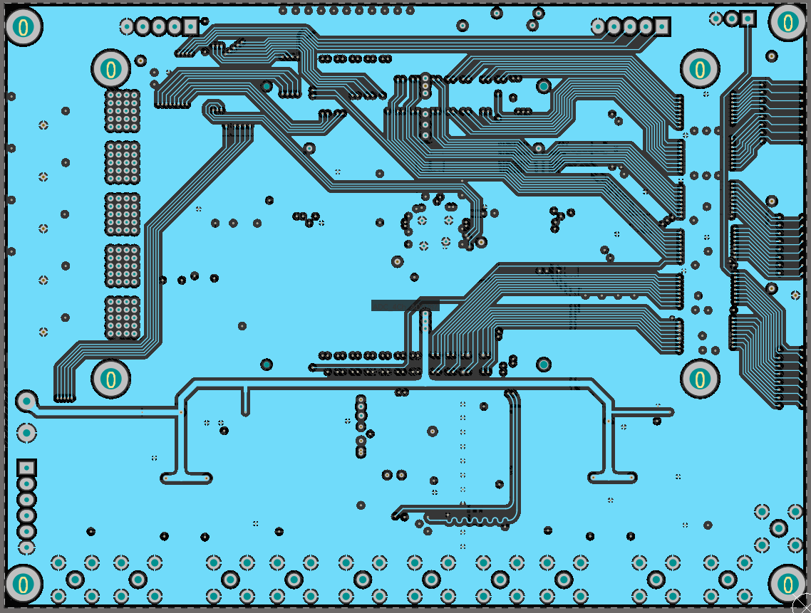
Here is 2D layer2 image of PCB on100MSPS High Speed ADC - 4 Channel
Here is 2D Bottom layer image of PCB on 100MSPS High Speed ADC - 4 Channel
Here is schematic of AD9287 ADC in board 100MSPS High Speed ADC - 4 Channel

Here is schematic of AD8332 ADC Bufffer in board 100MSPS High Speed ADC - 4 Channel

Here is schematic of ADT1-1WT input Buffer in board 100MSPS High Speed ADC - 4 Channel

Here is schematic of AD9515 Clock buffer in board 100MSPS High Speed ADC - 4 Channel

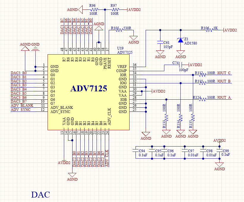
Here is schematic of ADV7125 DAC in board 100MSPS High Speed ADC - 4 Channel
Here is schematic of DAC buffer in board 100MSPS High Speed ADC - 4 Channel

Here is result of data read by AD9287, 8 bit
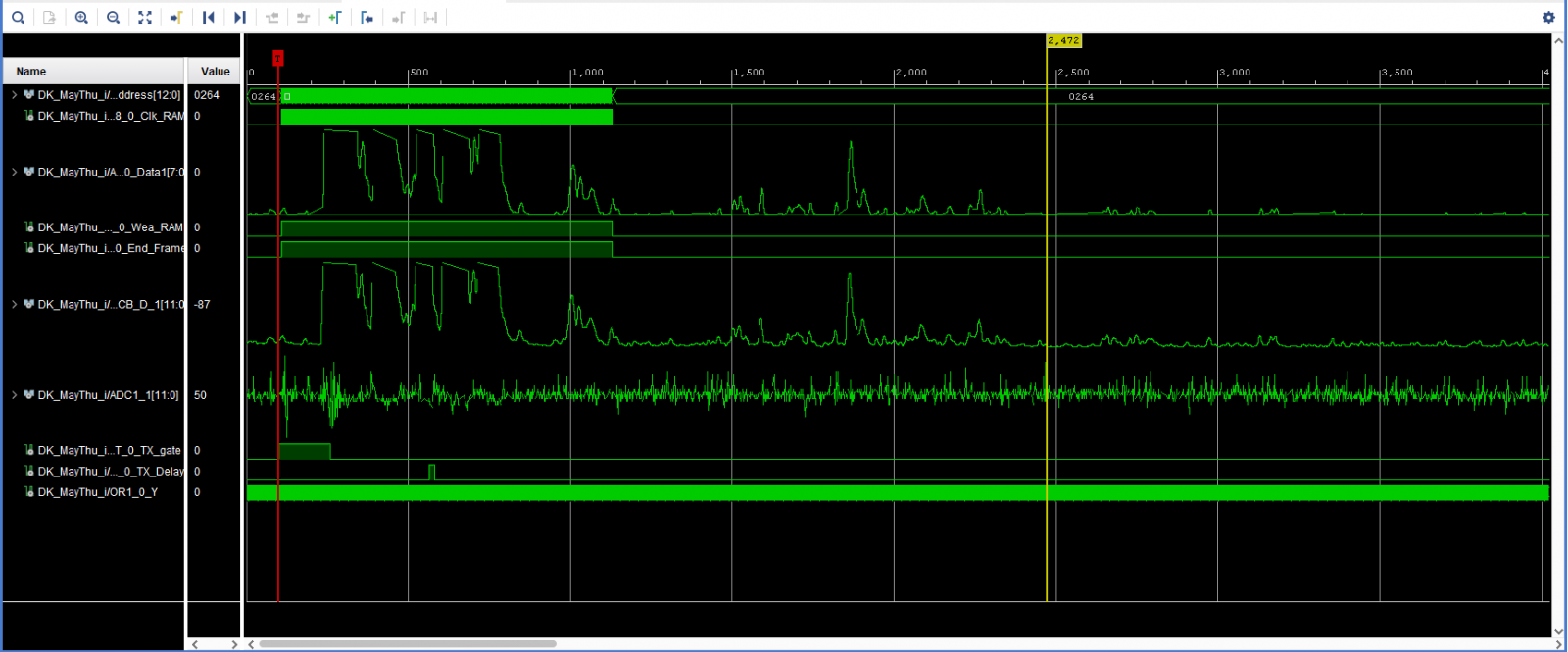
Here is result of data read by AD9287 and demodulation
