Tutorial Overview
In the ISE/EDK tools, we’d use the Base System Builder to generate a base project for a particular hardware platform. Now with Vivado, the process is a little different but we have more control in how things are setup and we still benefit from some powerful automation features. In this tutorial we’ll create a base design for the Zynq in Vivado and we’ll use the MicroZed board as the hardware platform.
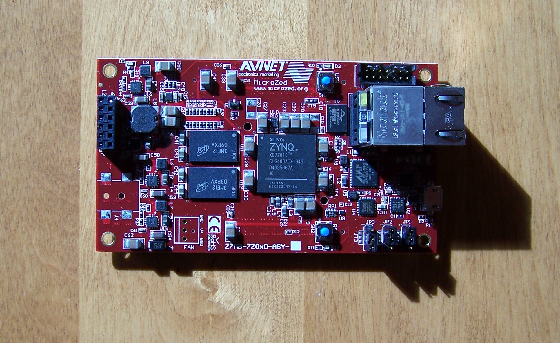
Requirements
Before following this tutorial, you’ll need the following:
-
Vivado 2014.2
-
MicroZed
-
Platform Cable USB II (or equivalent JTAG programmer)
Create a new Vivado project
Follow these steps to create a new project in Vivado:
-
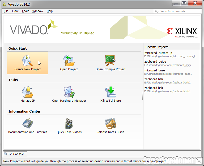
Open Vivado. From the welcome screen, click “Create New Project”.
-
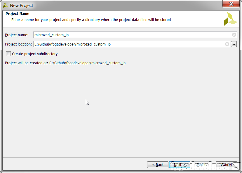
Specify a folder for the project. I’ve created a folder named “microzed_custom_ip”. Click “Next”.
-
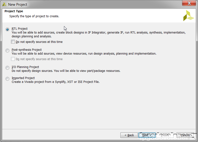
For the Project Type window, choose “RTL Project”. Click “Next”.
-
For the Add Sources window, click “Next”. We will add our multiplier source code later.
-
For the Add Existing IP window, click “Next”.
-
For the Add Constraints window, click “Next”.
-
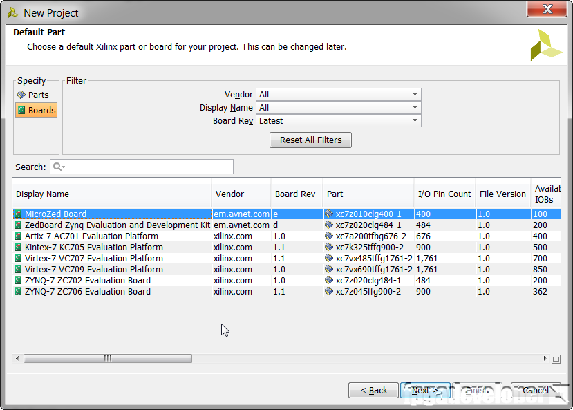
For the Default Part window, select the “MicroZed Board” and click “Next”.
-
Click “Finish” to complete the new project wizard.
Change the project’s default language
By default, the project will be created using Verilog as the default language. As we’ll be importing VHDL, let’s change that to VHDL:
-
From the menu, select Tools->Options.
-
In the “General” tab select target language : VHDL.
Setup the Zynq PS
The new Vivado project starts off blank, so to create a functional base design, we need to at least add the Zynq PS (processor system) and make the minimal required connections. Follow these steps to add the PS to the project:
-
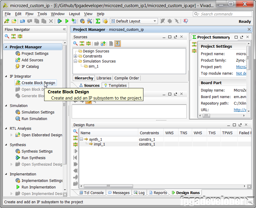
From the Vivado Flow Navigator, click “Create Block Design”.
-
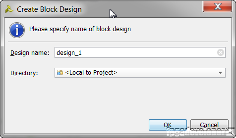
Specify a name for the block design. Let’s go with the default “design_1” and leave it local to the project. Click “OK”.
-
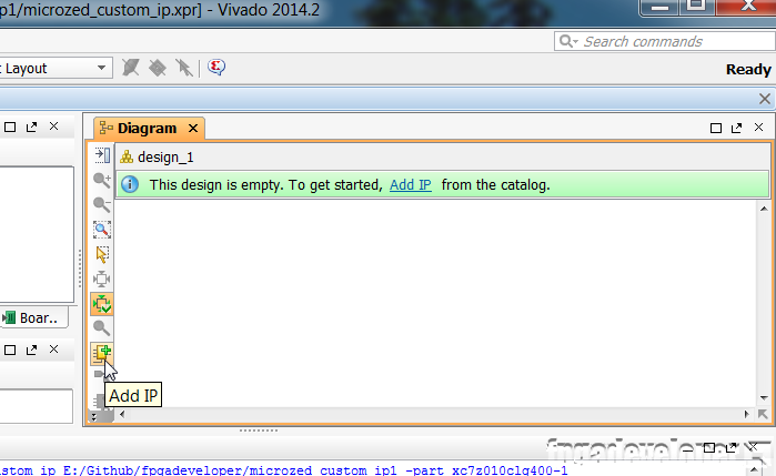
In the Block Design Diagram, you will see a message that says “This design is empty. To get started, Add IP from the catalog.”. Follow this advice by clicking on the blue “Add IP” link, or by using the “Add IP” icon.
-
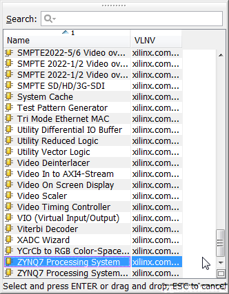
The IP catalog should appear. Go to the end of the list and double click on the block named “ZYNQ7 Processing System” – it should be the second last on the list. Vivado will now add the PS to the block diagram.
-
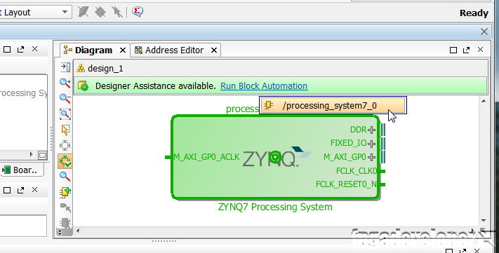
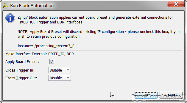
In the Block Design Diagram, you will see a message that says “Designer Assistance available. Run Block Automation”. Click on the “Run Block Automation” link and select “processing_system7_0” from the drop-down menu. Block Automation makes connections and pin assignments to external hardware such as the DDR and fixed IO. It does this using the board definition of the hardware platform you specified when you created the project (MicroZed). We could make these connections ourselves if we were using a custom board, but for off-the-shelf boards, Block Automation makes the process a lot easier.
-
In the Block Automation window, make sure “Apply Board Preset” is ticked and click “OK”.
-
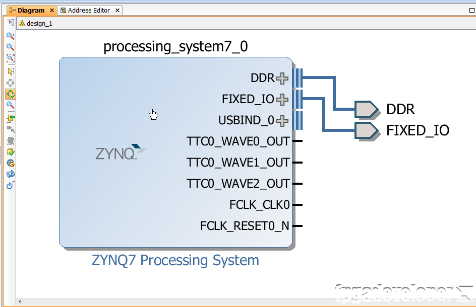
Now our block diagram has changed and we can see that the DDR and FIXED_IO are connected externally. Now the only remaining connection to make is the clock that we will use for the AXI buses. We must configure the Zynq to generate a clock and enable a general purpose AXI bus. To make these settings, double click on the Zynq PS block.
-
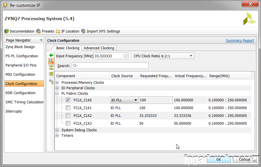
The Re-customize IP window will open. From the Page Navigator, select “Clock Configuration” and open the “PL Fabric Clocks” tree.
-
Make sure that the FCLK_CLK0 is enabled (ticked) and that it is set for a frequency of 100MHz. This will be our AXI clock.
-
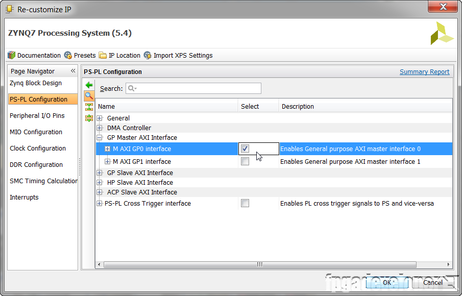
Now from the Page Navigator, select “PS-PL Configuration” and open the “GP Master AXI Interface” tree.
-
Tick the “M AXI GP0 interface” checkbox to enable it.
-
Now click “OK” to close the Re-customize IP window.
-
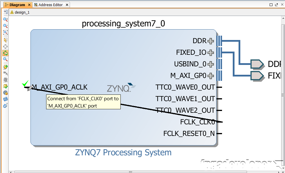
You should now see a new input port on the left side of the Zynq PS block. This is the AXI clock input.
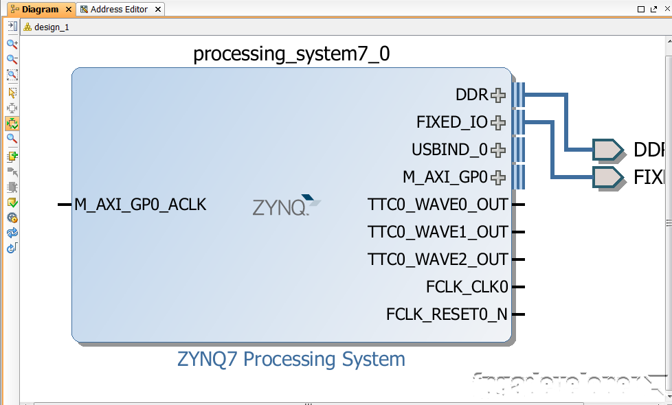 We must now connect the FCLK_CLK0 output to the AXI clock input. To do this, click on the FCLK_CLK0 output and then click on the M_AXI_GP0_ACLK input. This will trace a wire between the pins and make the connection.
Create the HDL wrapper
Now the Zynq is setup and all we need to do to create a functional project is to create a HDL wrapper for the design.
-
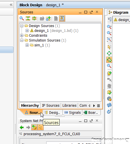
Open the “Sources” tab from the Block Design window.

-
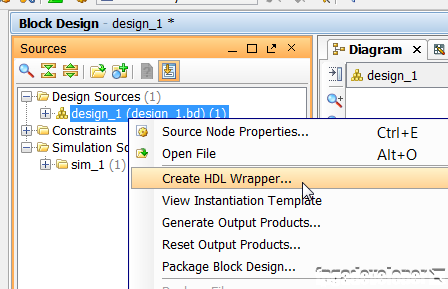
Right-click on “design_1” and select “Create HDL wrapper” from the drop-down menu.

-
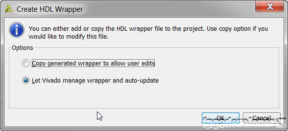
From the “Create HDL wrapper” window, select “Let Vivado manage wrapper and auto-update”. Click “OK”.

From this point, we have a base design containing the Zynq PS from which we could generate a bitstream and test on the MicroZed. We haven’t exploited any of the FPGA fabric, but the Zynq PS is already connected to the Gigabit Ethernet PHY, the USB PHY, the SD card, the UART port and the GPIO, all thanks to the Block Automation feature. So there is already quite a lot we could do with the design at this point, such as running Linux on the PS or running a bare metal application on it.
Generate the bitstream
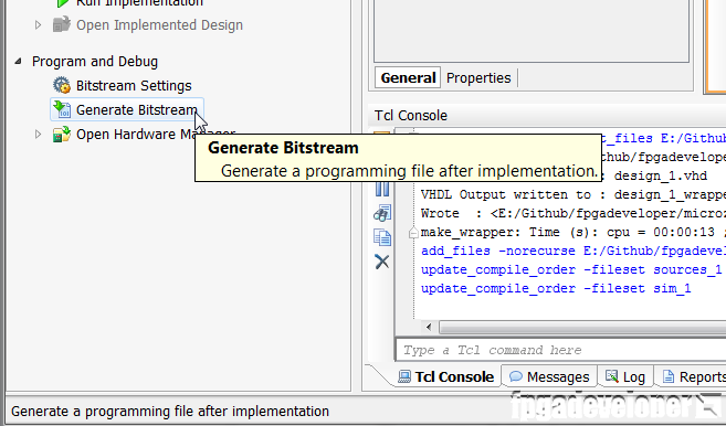
To generate the bitstream, click “Generate Bitstream” in the Flow Navigator.
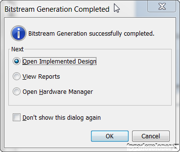
Once the bitstream is generated, the following window appears. Select “Open Implemented Design” and click “OK”.

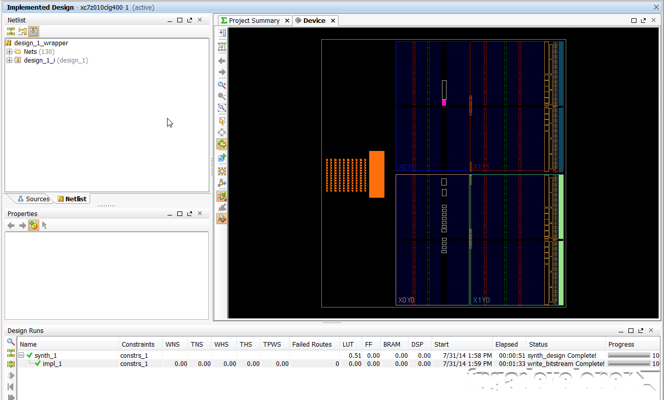
The implemented design will open in Vivado showing you a map of the Zynq device and how the design has been placed. In our case, we haven’t used any of the FPGA fabric (only the PS), so the map is empty for the most part.

Export the hardware to SDK
Once the bitstream has been generated, the hardware design is done and we’re ready to develop the code to run on the processor. This part of the design process is done in Xilinx Software Development Kit (SDK), so from Vivado we must first export the project to SDK.
-
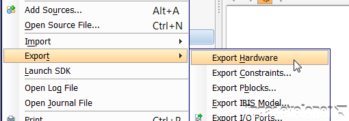
In Vivado, from the File menu, select “Export->Export hardware”.

-
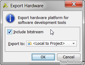
In the window that appears, tick “Include bitstream” and click “OK”.

-
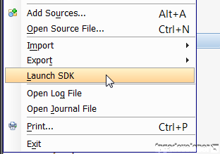
Again from the File menu, select “Launch SDK”.

-
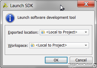
In the window that appears, use the following settings and click “OK”.

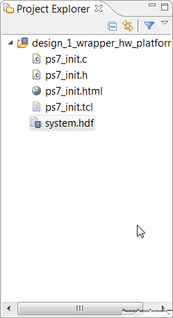
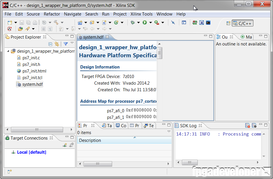
At this point, the SDK loads and a hardware platform specification will be created for your design. You should be able to see the hardware specification in the Project Explorer of SDK as shown in the image below.

You are now ready to create a software application to run on the PS.
Create a Software application
At this point, your SDK window should look somewhat like this:

To demonstrate creating an application for the Zynq, we’ll create a hello world application that will send “hello world” out the UART and to our PC.
-
From the File menu, select New->Application Project.

-
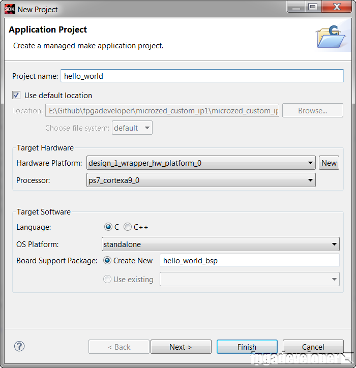
In the first page of the New Project wizard, choose a name for the application. I’ve chosen
hello_world. Click “Next”.
-
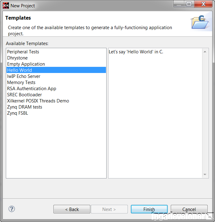
On the templates page, select the “Hello World” template and click “Finish”.

-
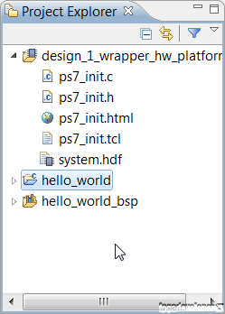
The SDK will generate a new application which you should find in the Project Explorer as in the image below.

The hello_world folder contains the software application, which you can browse and modify. I suggest you take a look at the code that is contained here and get familiar with it.
The hello_world_bsp folder contains the Board Support Package, which is a bunch of libraries that are provided for accessing the various peripherals and features of the Zynq. In general, it’s better not to modify this code because it gets written over every time you use the “Clean project” option. Instead, if you want to make customizations, try to keep it in the application folder.
Once the software application has been created, it is automatically built. Once the application is built, we are ready to test the design on hardware.
Test the design on the hardware
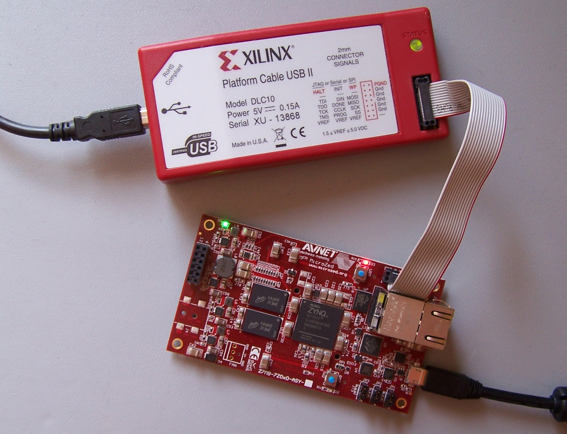
To test the design, we are using the MicroZed board from Avnet. Make the following setup before continuing:
-
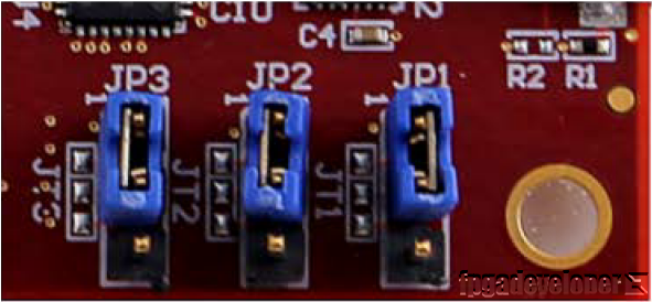
On the MicroZed, set the JP1, JP2 and JP3 jumpers all to the 1-2 position.

-
Connect the USB-UART (J2) to a USB port of your PC.
-
Connect a Platform Cable USB II programmer (or similar device) to the JTAG connector. Connect the programmer to a USB port of your PC.

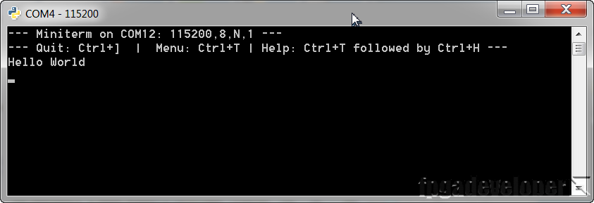
Now you need to open up a terminal program on your PC and set it up to receive the “hello world” message. I use Miniterm because I’m a Python fan, but you could use any other terminal program such as Putty. Use the following settings:
-
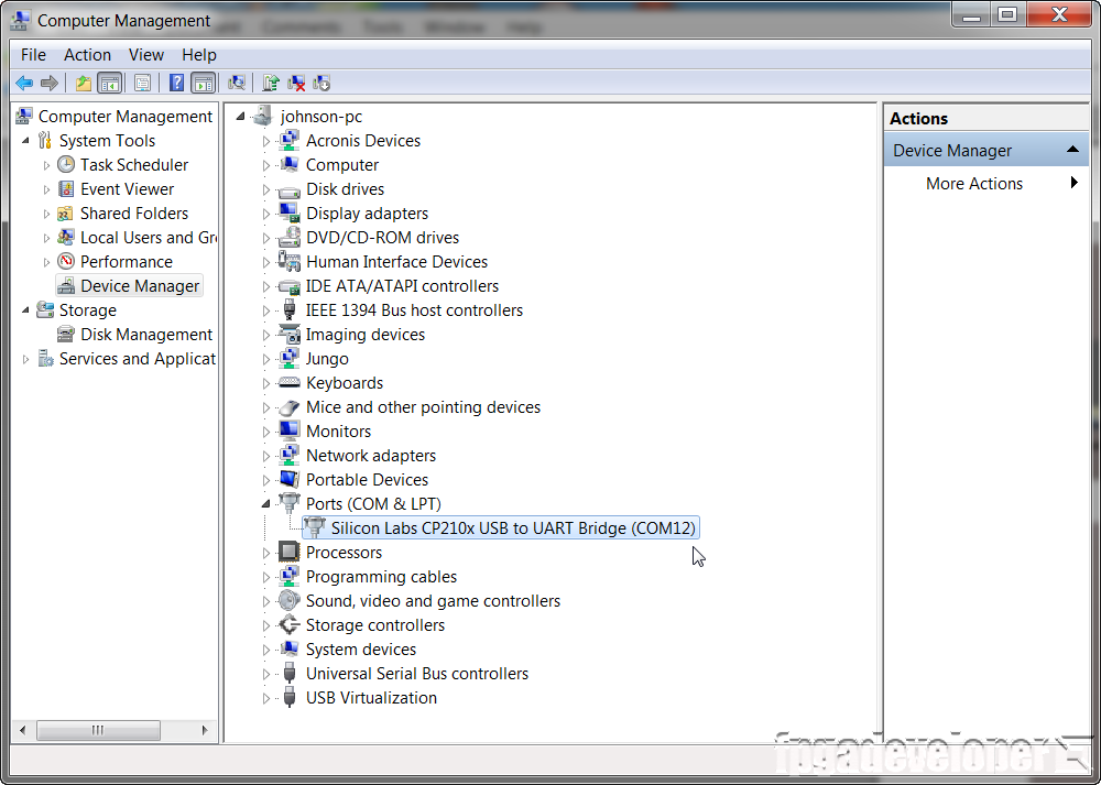
Comport - check your device manager to find out what comport the MicroZed popped up as. In my case, it was COM12 as shown below.

-
Baud rate: 115200bps
-
Data: 8 bits
-
Parity: None
-
Stop bits: 1
Now that your PC is ready to receive the “hello world” message, we are ready to send our bitstream and software application to the hardware.
-
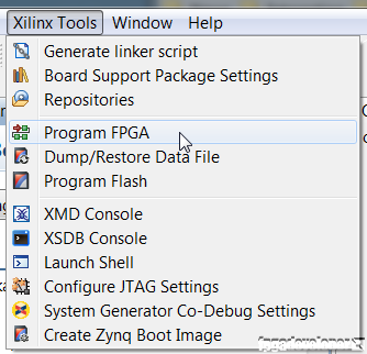
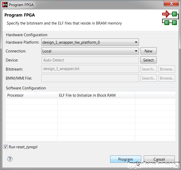
In the SDK, from the menu, select Xilinx Tools->Program FPGA.

-
In the Program FPGA window, we select the hardware platform to program. We have only one hardware platform, so click “Program”.

-
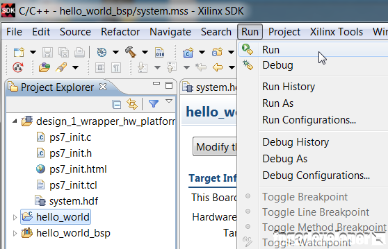
The bitstream will be loaded onto the Zynq and we are ready to load the software application. Select the
hello_world folder in the Project Explorer, then from the menu, select Run->Run.
-
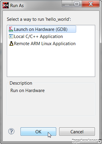
In the Run As window, select “Launch on Hardware (GDB)” and click “OK”.

-
The application will be loaded on the Zynq PS and it will be executed. Look out for the “Hello World” message in your terminal window!

What now?
In the following tutorials I’ll go through more concepts such as:
-
Creating a custom IP block and integrating your own HDL code
-
Using the DMA engine for transferring data between IP and memory
-
Running Linux on the PS
-
Accessing IP through a Linux application
Source code
The TCL build script and source code for this project is shared on Github here:
https://github.com/fpgadeveloper/microzed-base
For instructions on rebuilding the project from sources, read my post on version control for Vivado projects.

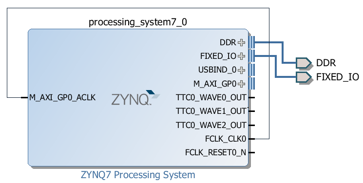


 We must now connect the FCLK_CLK0 output to the AXI clock input. To do this, click on the FCLK_CLK0 output and then click on the M_AXI_GP0_ACLK input. This will trace a wire between the pins and make the connection.