This is the first part of a three part tutorial series in which we will go through the steps to create a PCI Express Root Complex design in Vivado, with the goal of being able to connect a PCIe end-point to our FPGA. We will test the design on hardware by connecting a PCIe NVMe solid-state drive to our FPGA using the FPGA Drive adapter.
In the first part of this tutorial series we will build a Microblaze based design targeting the KC705 Evaluation Board. In the second part, we will build a Zynq based design targeting the PicoZed 7Z030 and PicoZed FMC Carrier Card V2. In part 3, we will test the design on the target hardware using a stand-alone application that will validate the state of the PCIe link and perform enumeration of the PCIe end-points. We will then run PetaLinux on the FPGA and prepare our SSD for use under the operating system.
Requirements
To complete this tutorial you will need the following:
Note: The tutorial text and screenshots are suitable for Vivado 2015.4 however the sources in the Git repository will be regularly updated to the latest version of Vivado.
The Components
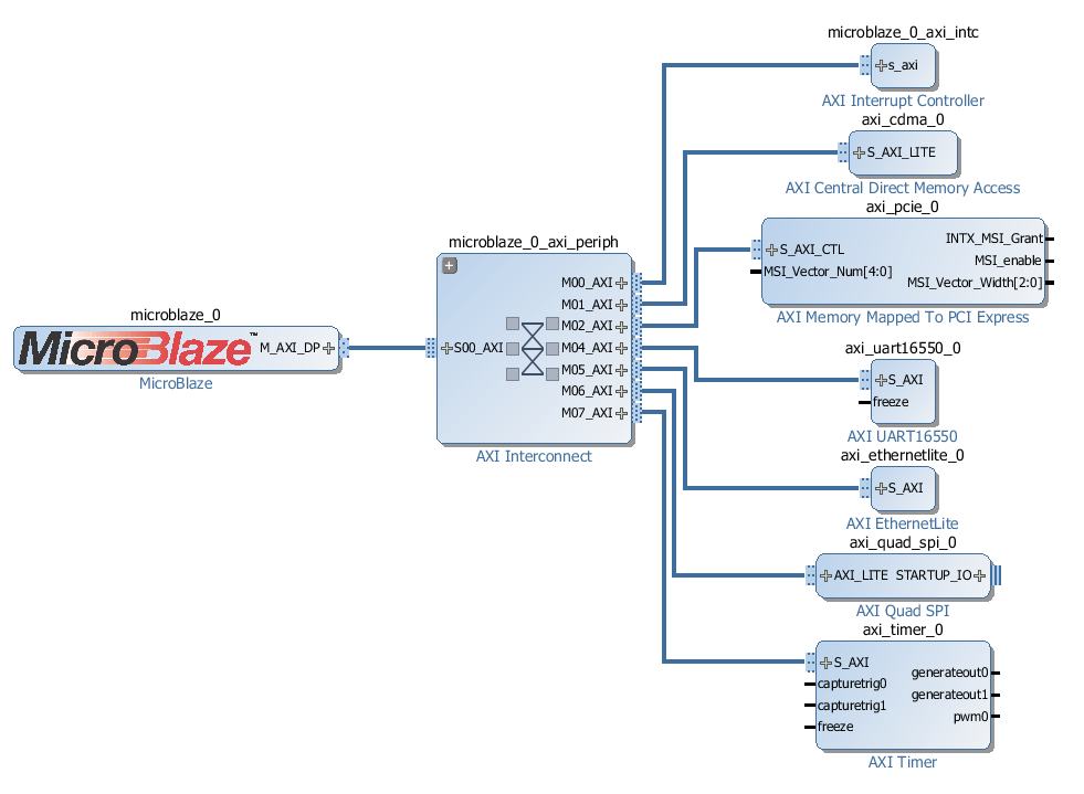
The image below gives us a high level view of the design showing each component and how it connects to the Microblaze - only the AXI-Lite interfaces are shown.

Let’s talk about the role of each peripheral in the design:
-
AXI Interrupt Controller - connects to the interrupts generated by the peripherals and routes them through to the Microblaze. It’s generally a good idea to connect all interrupts to the Microblaze when you plan to run PetaLinux.
-
AXI Central DMA - performs data transfers from one memory mapped space to another. We have the CDMA in this design to be able to make fast data transfers between the PCIe end-point and the DDR3 memory.
-
AXI Memory Mapped to PCI Express - performs address mapping between the AXI address space and the PCIe address space. It contains the integrated PCI Express block and all the logic required to translate PCIe TLPs into AXI memory mapped reads and writes. The AXI-PCIe block has a slave interface (S_AXI) to allow an AXI master (such as the Microblaze) to access the PCIe address space, and it also has a master interface (M_AXI) which allows a PCIe end-point to access the AXI address space.
-
AXI UART16550 - UART for console output, which is needed by our stand-alone software application and by PetaLinux.
-
AXI EthernetLite - provides a 10/100Mbps network connection for PetaLinux.
-
AXI Quad SPI - provides access to a QSPI Flash device which can be used for storing software, the Linux kernel or FPGA configuration files.
-
AXI Timer - provides an accurate timer needed by PetaLinux.
The Address Spaces
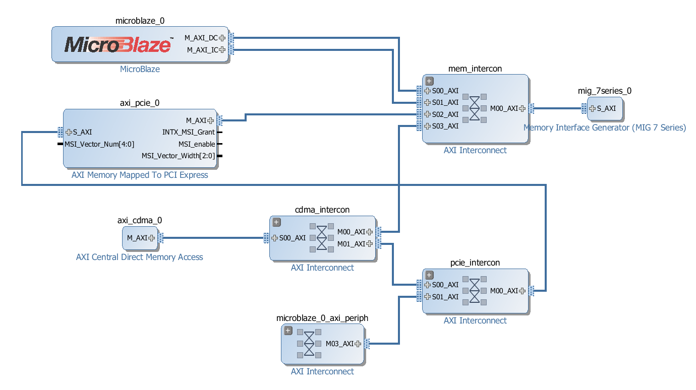
The image below shows the AXI memory mapped interface connections which is useful for understanding the memory spaces and the devices that have access to them.

The important thing is to understand is who the bus masters are and what address spaces they can access - the connections could have been made in a number of different ways to achieve the same goal.
The 2 address spaces are:
-
the DDR3 memory accessed through the MIG, and
-
the PCIe address space accessed through the S_AXI interface of the AXI-PCIe bridge
The 3 AXI masters and the address spaces they can access are:
-
the Microblaze can access both the DDR3 memory and the PCIe address space
-
the PCIe end-point with bus mastering capability can access the DDR3 memory only (via M_AXI port of the AXI-PCIe bridge)
-
the CDMA can access both the DDR3 memory and the PCIe address space
About PCIe end-point bus mastering
Most PCIe end-points have bus mastering capability. Basically this means that the PCIe end-point can send memory read/write TLPs to the root complex and read/write to a part of the system memory that was allocated for the end-point. Maybe the most common application of end-point bus mastering is the implementation of Message Signaled Interrupts (or MSI). When a PCIe end-point generates an MSI, it simply writes to part of the system memory that was allocated by the root complex.
Create a new Vivado project
We start by creating a new project in Vivado and selecting the KC705 Evaluation board as our target.
-
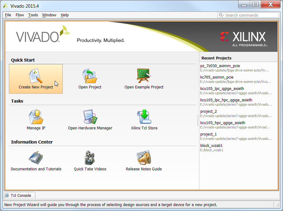
From the welcome screen, click “Create New Project”.

-
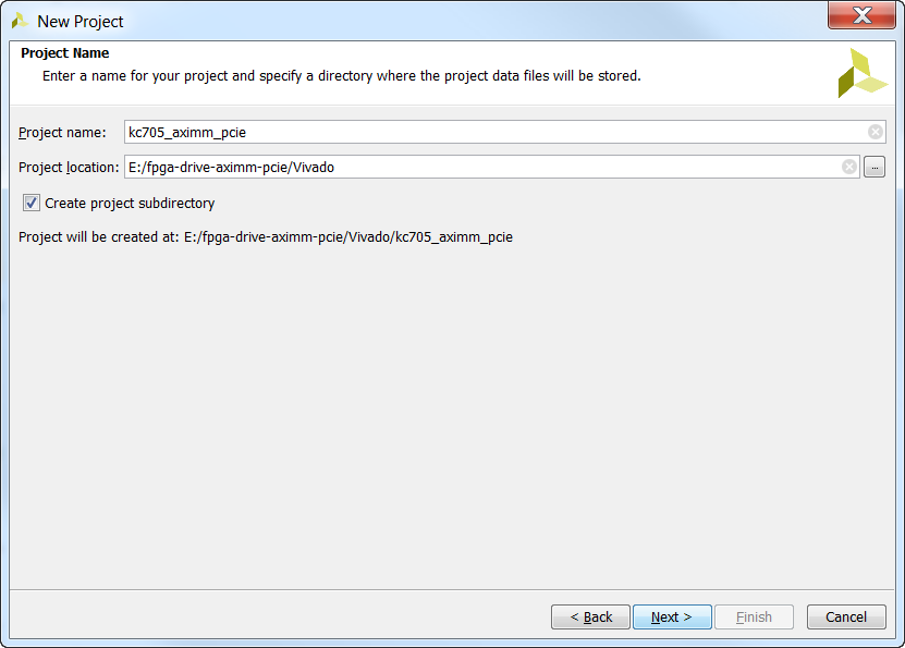
Specify a folder for the project. I’ve created a folder named “kc705_aximm_pcie”. Click “Next”.

-
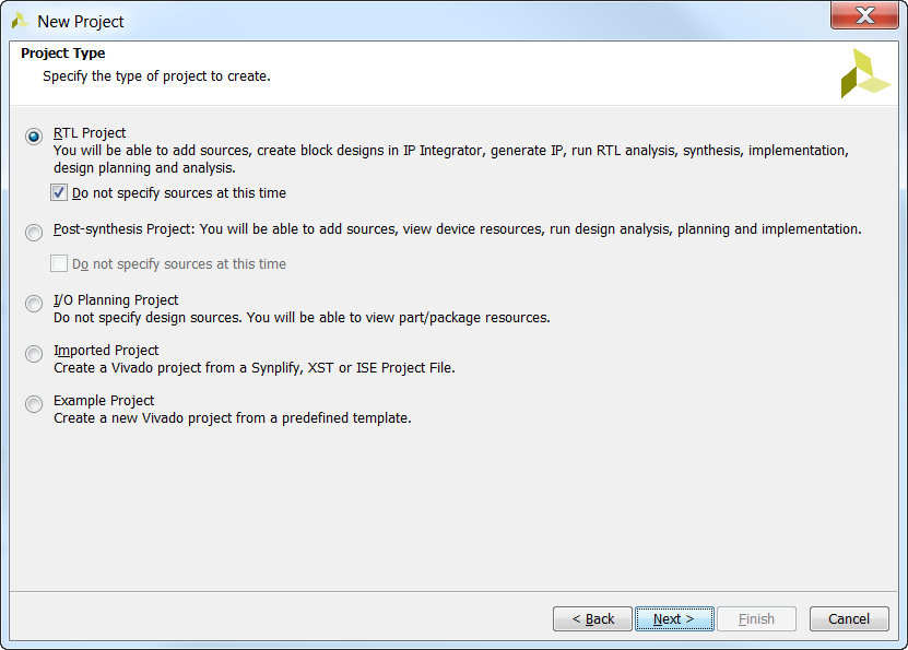
For the Project Type window, choose “RTL Project” and tick “Do not specify sources at this time”. Click “Next”.

-
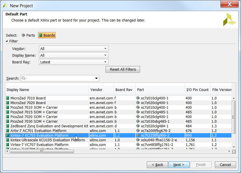
For the Default Part window, select the “Boards” tab and then select the “Kintex-7 KC705 Evaluation Platform” and click “Next”.

-
Click “Finish” to complete the new project wizard.
Create the block design
Now we need to create and build our block design. We will start by adding the Microblaze and the AXI Memory Mapped PCI Express Bridge.
-
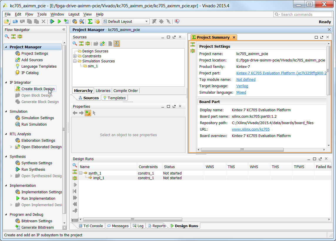
From the Vivado Flow Navigator, click “Create Block Design”.

-
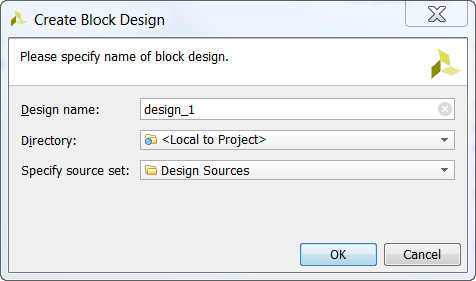
Specify a name for the block design. Let’s go with the default “design_1” and leave it local to the project. Click “OK”.

-
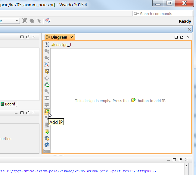
In the Block Design Diagram, you will see a message that says “This design is empty. Press the (Add IP) button to add IP.”. Click on the “Add IP” icon either in the message, or in the vertical toolbar.

-
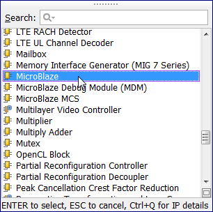
The IP catalog will appear. Find and double click on “Microblaze”.

-
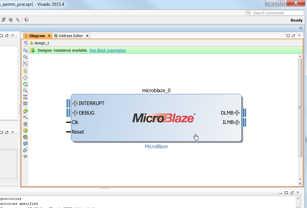
You will see the Microblaze in the block diagram. Double click on it to open the configuration wizard.

-
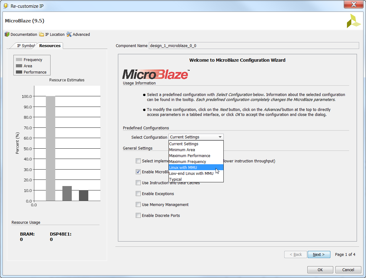
The Microblaze has several predefined configurations that can be selected on the first page of the Microblaze Configuration Wizard. We eventually want to run PetaLinux on the Microblaze, so we need to select “Linux with MMU” to get the best configuration for that. Then click “OK” to accept that configuration.

-
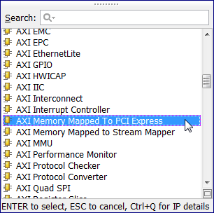
The AXI-PCIe block is going to provide the clock source for most of our design, including the Microblaze. By adding it to our block design at this point, we will then be able to use the Block Automation feature to setup a lot of the required hardware, saving us a lot of time. Find the “AXI Memory Mapped to PCI Express Bridge IP” in the IP Catalog and double click on it to add it to the block diagram.

-
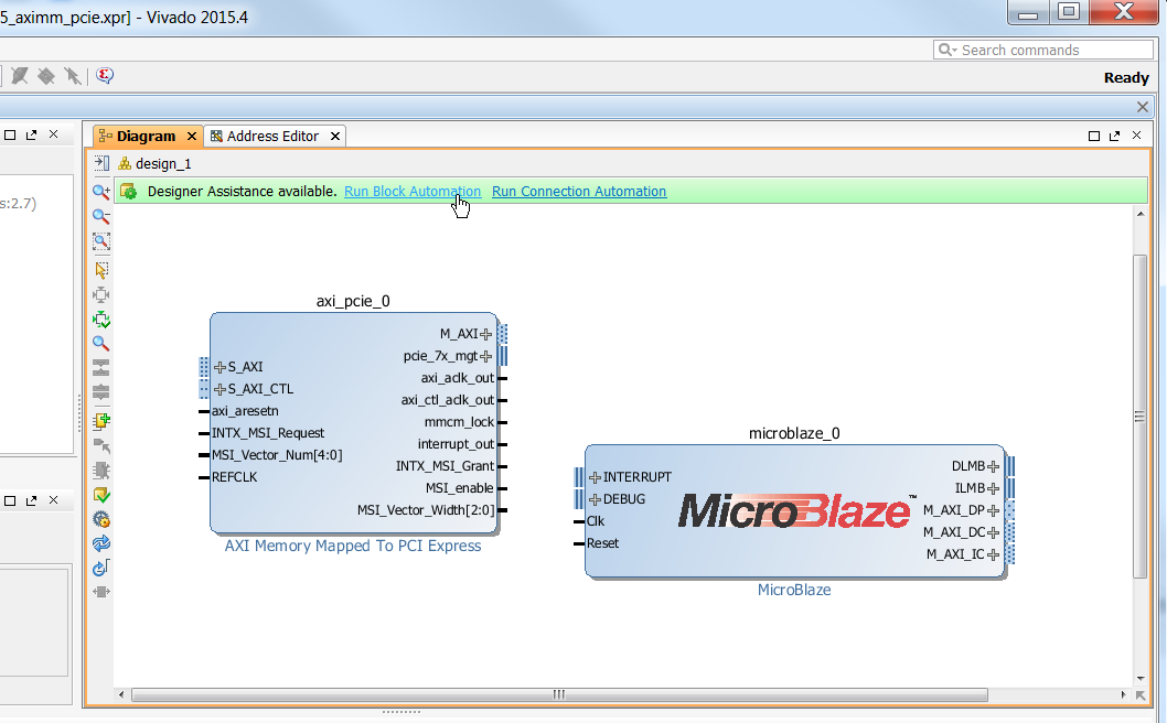
Now click on “Run Block Automation” which will help us to setup the Microblaze local memory, the Microblaze MDM, the Processor System Reset and the AXI Interrupt Controller.

-
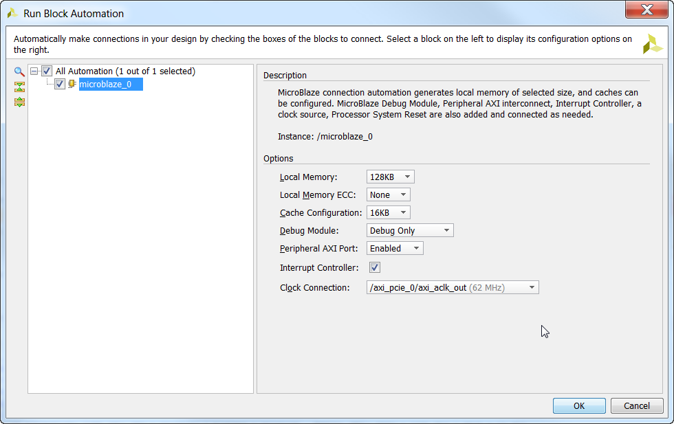
In the Run Block Automation window, apply the settings shown in the image below. Set the Local Memory to 128KB. Set the Cache Configuration to 16KB. Tick the Interrupt Controller checkbox. Set the Clock Connection to
/axi_pcie_0/axi_aclk_out. Then click OK.
-
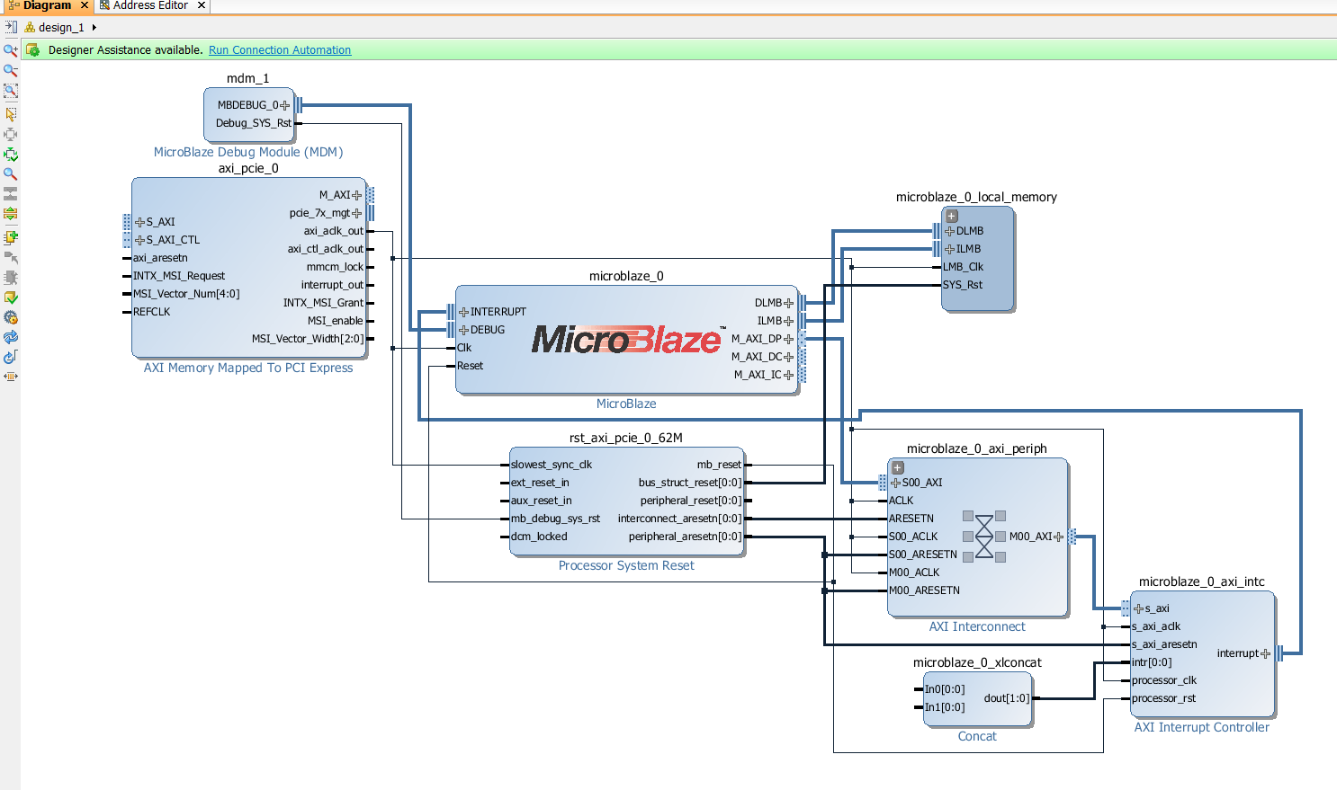
The block diagram should now look like the image below. Notice that everything so far is driven by the
axi_aclk_out clock which is driven by the AXI-PCIe block. The reset signals are generated by the Processor System Reset block, which will synchronize the external reset pushbutton signal to the axi_aclk_out clock.
-
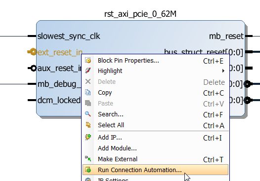
Right click on the
ext_reset_in input of the rst_axi_pcie_0_62M Processor System Reset and select “Run Connection Automation”, then click OK. This will connect the reset input to the KC705’s reset pushbutton.
Add the MIG
-
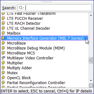
Now let’s add the DDR3 memory to the design. Find the “Memory Interface Generator (MIG 7 series)” in the IP Catalog and double click it to add it to the block diagram.

-
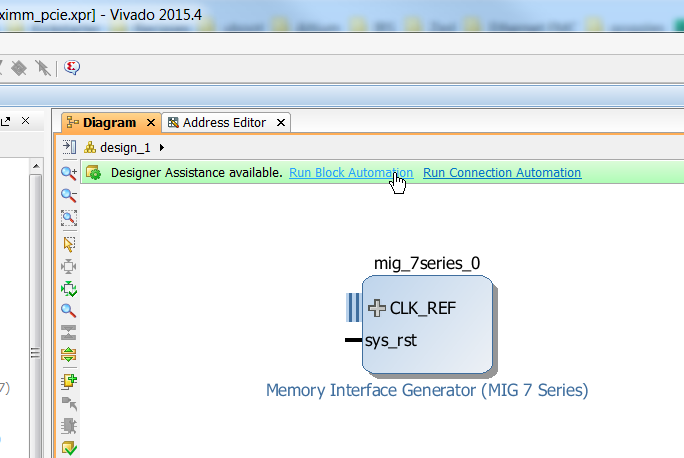
Click “Run Block Automation” to setup the external connections to the MIG.

-
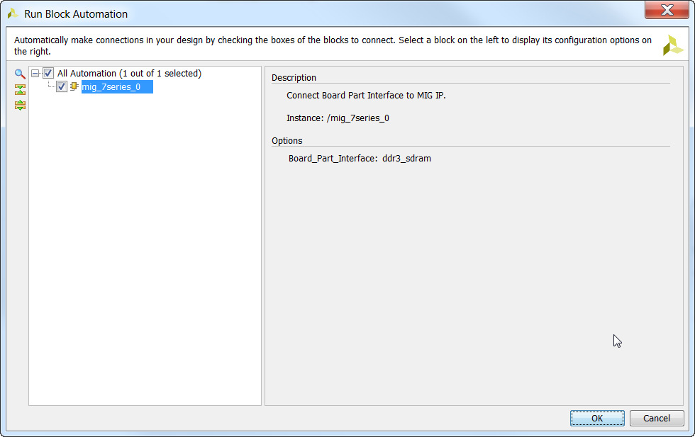
In the Run Block Automation window, click “OK”.

-
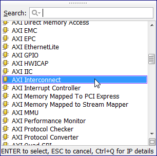
The connection automation feature can save us a lot of time setting up the MIG, but if we run it now, Vivado will connect it to the Microblaze through the AXI Interconnect that is already in the design (microblaze_0_axi_periph). There’s nothing particularly wrong with that, but in this design we want to have a separate AXI Interconnect for the MIG so that we can more easily control which blocks have access to the DDR3 and which have access to the peripherals. It’s a point to consider in this design because we will have a PCIe end-point with bus mastering capabilities, and we need to limit what the end-point will have access to. Find “AXI Interconnect” in the IP Catalog and double click on it to add one to the design.

-
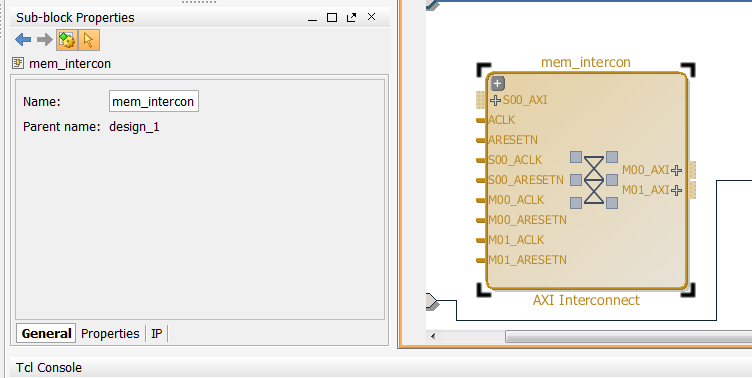
Click on the AXI Interconnect block and rename it to
mem_intercon using the “Sub-block properties” window.
-
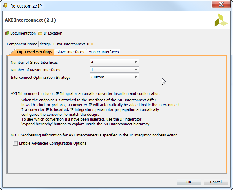
Double click on the
mem_intercon block and configure it for 4 slave interfaces, and 1 master interface.
-
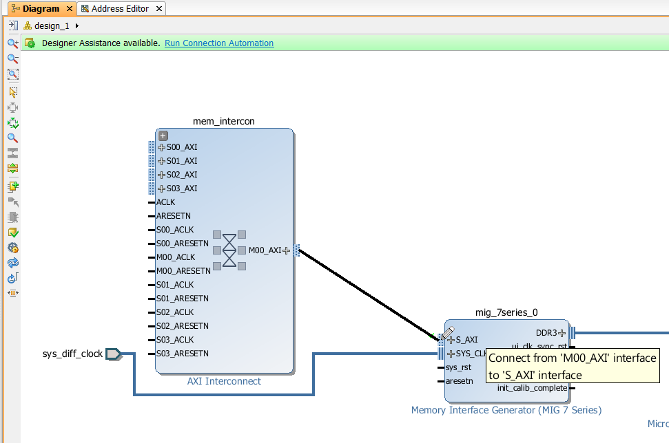
Connect the master interface (M00_AXI) of
mem_intercon to the slave interface (S_AXI) of the MIG.
-
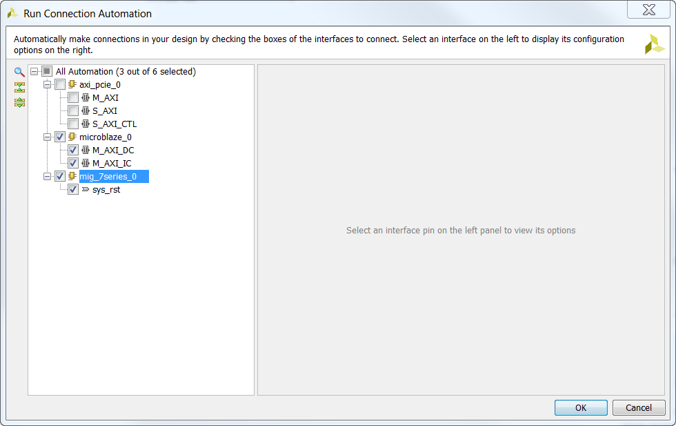
Now we can run the connection automation feature. Click “Run Connection Automation”. Select ONLY the
microblaze_0/M_AXI_DC, microblaze_0/M_AXI_IC and mig_7series_0/sys_rst connections. Click “OK”.
-
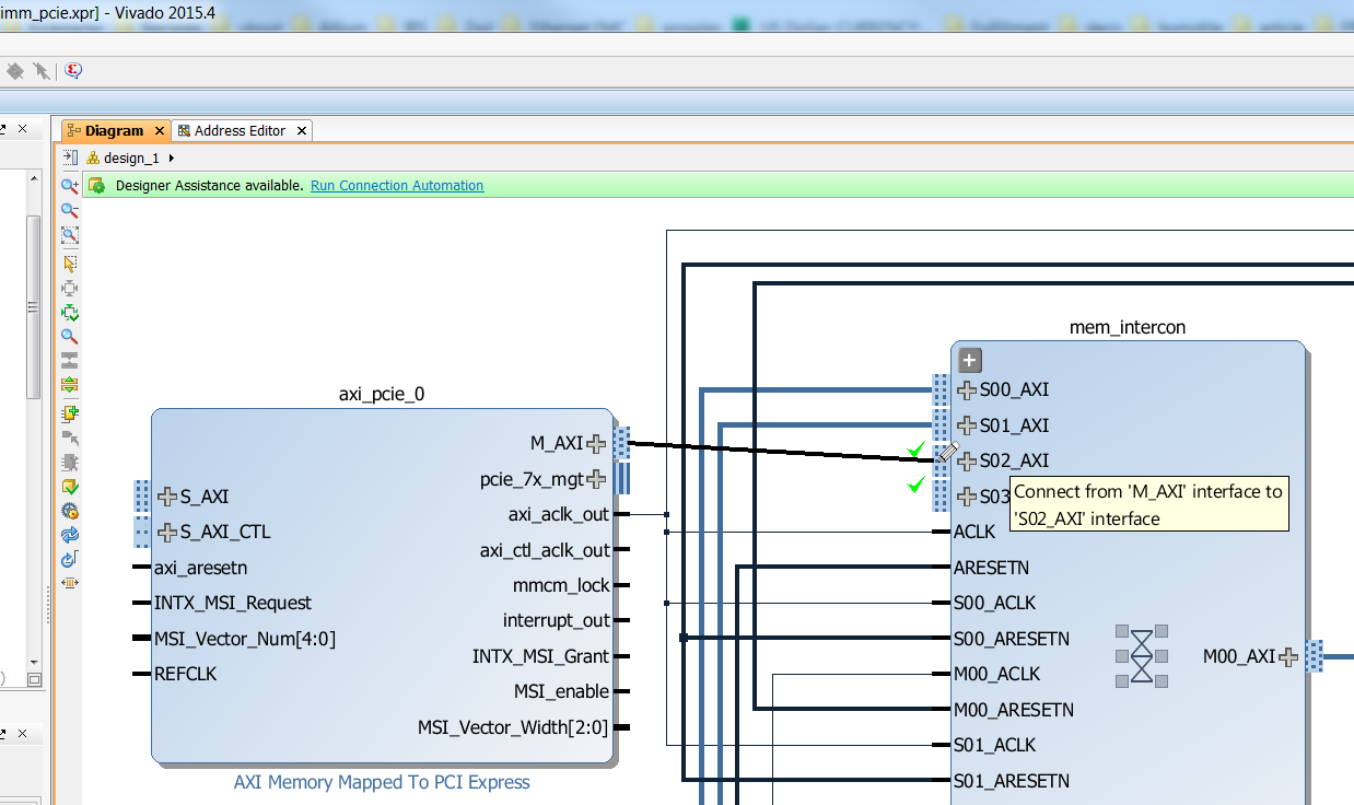
Connect the master interface (M_AXI) of
axi_pcie_0 to the slave interface (S02_AXI) of the mem_intercon. This provides a data path from the PCIe end-point to the DDR3 memory. Note that the PCIe end-point will not be able to access anything else in our design.
-
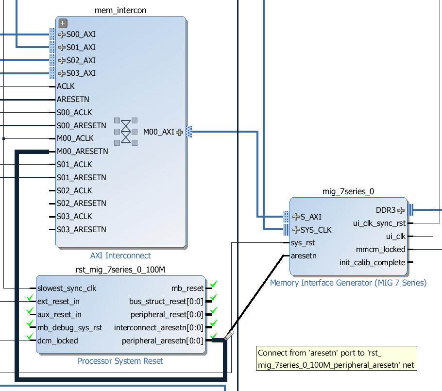
Connect the “aresetn” input of the MIG to the
peripheral_aresetn output of the rst_mig_7series_0_100M Processor System Reset block. Note that this Processor System Reset was generated when we used the connection automation feature in the steps above.
-
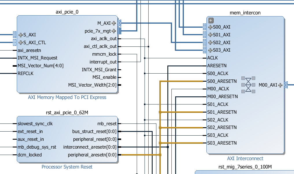
As shown in the image below, connect the
S02_ACLK and S03_ACLK clock inputs of the mem_intercon to the axi_aclk_out output of the AXI-PCIe block. Also connect the S02_ARESETN and S03_ARESETN inputs to the peripheral_aresetn of the rst_axi_pcie_0_62M Processor System Reset.
-
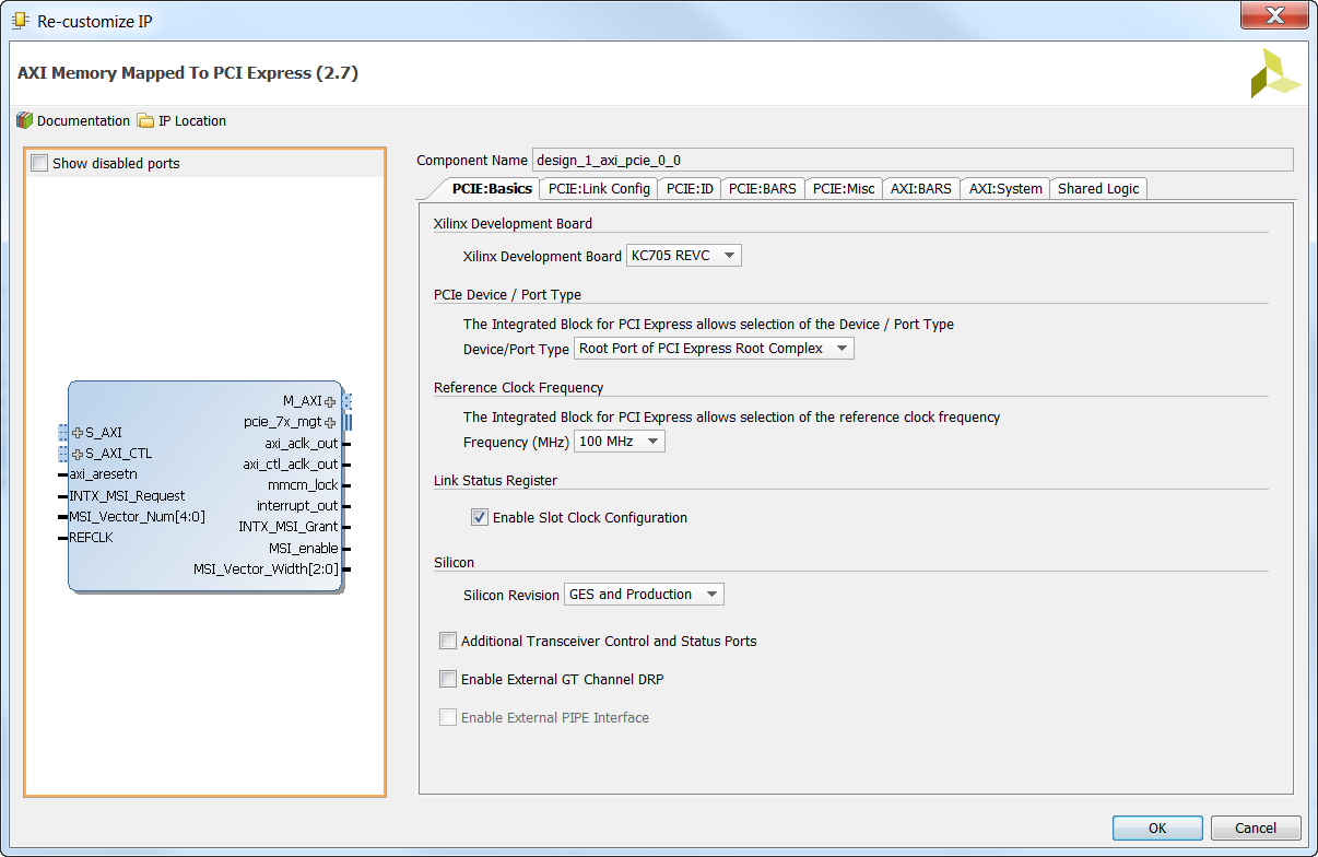
Double click on the AXI-PCIe block so that we can configure it. On the “PCIE:Basics” tab of the configuration, select “KC705 REVC” as the Xilinx Development Board, and select “Root Port of PCI Express Root Complex” as the port type.

-
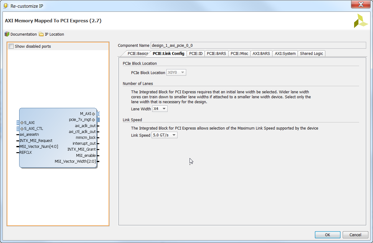
On the “PCIE:Link Config” tab, select a “Lane Width” of 4x and a “Link speed” of 5 GT/s (Gen2). Note that the KC705 has 8 lanes routed to the PCIe edge-connector, however the PCIe SSD that we want to connect with has only 4 lanes.

-
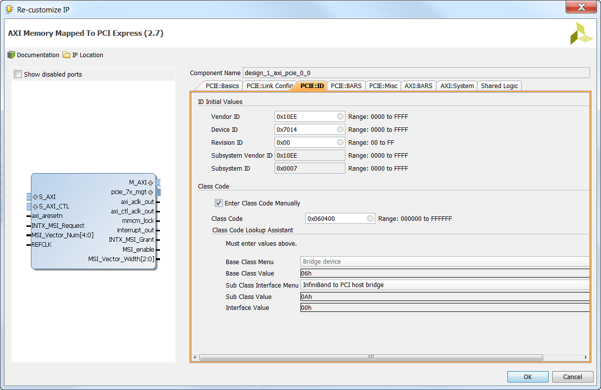
In the “PCIE:ID” tab, enter a “Class Code” of 0x060400. This is important for the last part of this tutorial series, in which we will be running PetaLinux. The class code will ensure that the correct driver is associated with the AXI to PCIe bridge IP.

-
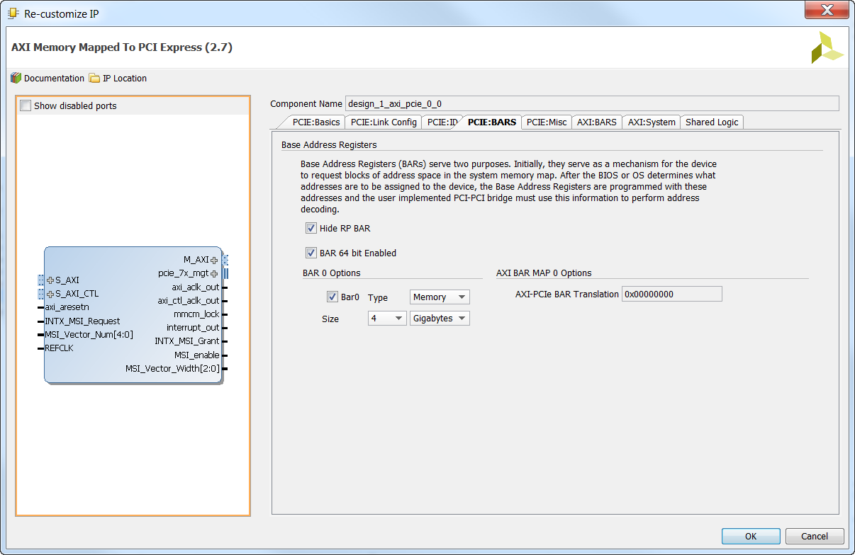
In the “PCIE:BARS” tab, tick “Hide RP BAR”, tick “BAR 64-bit Enabled” and set BAR 0 with type “Memory” and a size of 4 Gigabytes. In this configuration, the PCIe end-point is given access to the entire 32-bit address space - remember though that it’s only physically connected to the DDR3 memory.

-
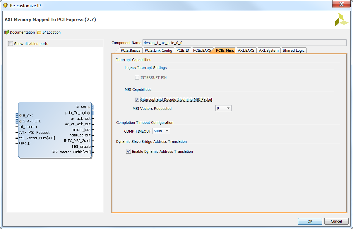
In the “PCIE:Misc” tab, use the defaults as shown in the image below.

-
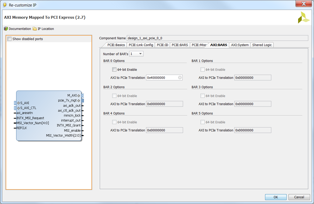
In the “AXI:BARS” tab, use the defaults as shown in the image below. We will later be able to configure the size of the AXI BAR 0 in the Address Editor.

-
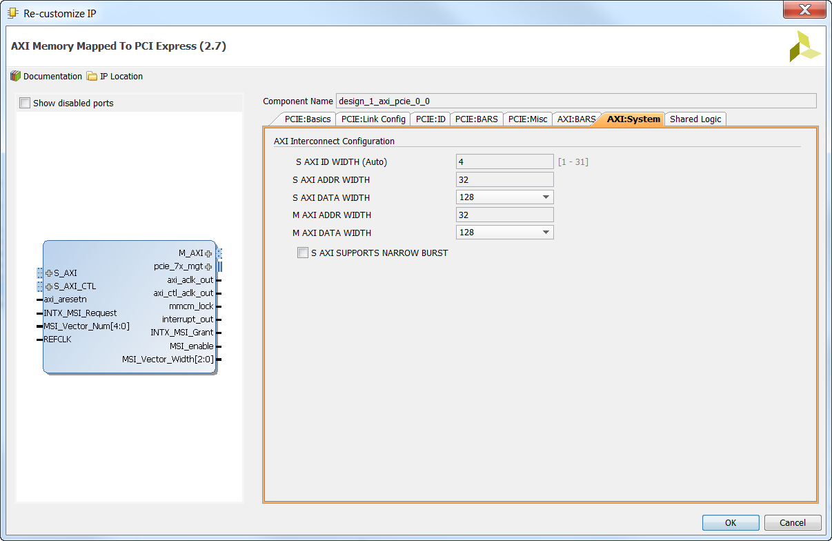
In the “AXI:System” tab, use the defaults as shown in the image below.

-
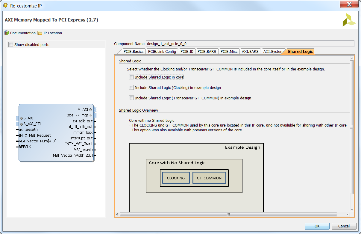
In the “Shared Logic” tab, use the defaults as shown in the image below. Click “OK”.

-
Right click on the
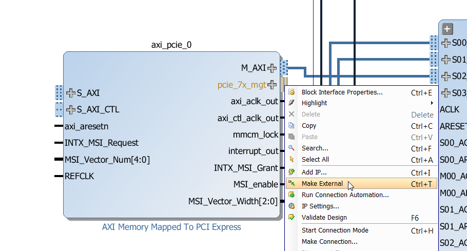
pcie_7x_mgt port of the AXI-PCIe block and select “Make External”. This will connect the gigabit transceivers to the 4 PCIe lanes on the PCIe edge-connector of the KC705.
-
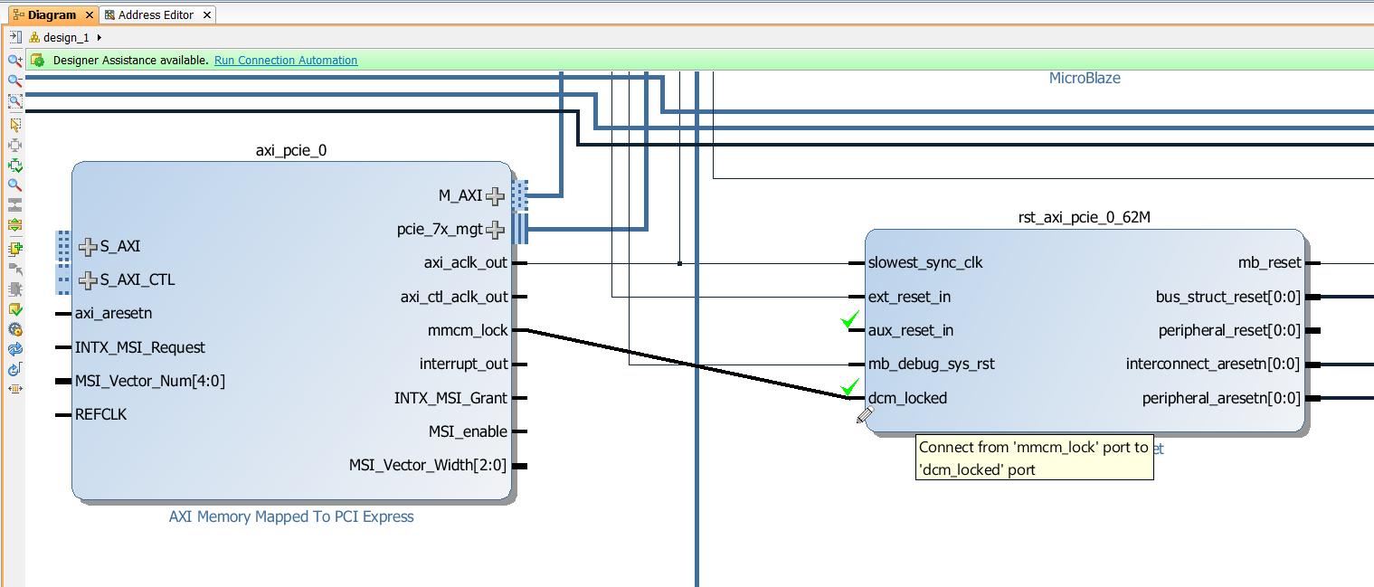
Connect the
mmcm_lock output of the AXI-PCIe block to the dcm_locked input of rst_axi_pcie_0_62M Processor System Reset block.
-
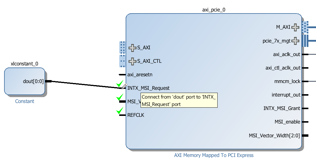
Add a “Constant” from the IP Catalog and configure it to output 0 (low). We’ll use this to tie low the
INTX_MSI_Request input of the AXI-PCIe block. Connect the constant’s output to the INTX_MSI_Request input of the AXI-PCIe block.
-
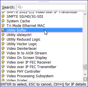
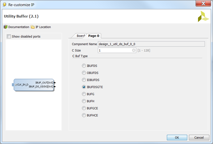
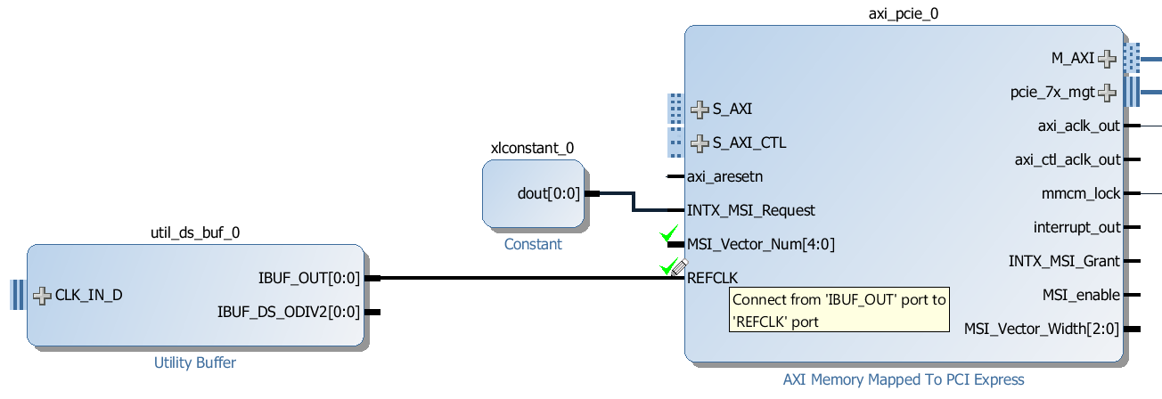
Add a “Utility Buffer” to the block design. This buffer is going to be connected to a 100MHz clock that will be provided to the KC705 board by the FPGA Drive adapter, via the PCIe edge-connector. A 100MHz reference clock is required by all PCIe devices.

-
Double click on the utility buffer and on the “Page 0” tab of the configuration window, select “IBUFDSGTE” as the C Buf Type. Click “OK”.

-
Connect the
IBUF_OUT output of the utility buffer to the “REFCLK” input of the AXI-PCIe block.
-
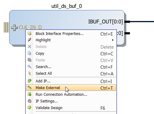
Right click on the
CLK_IN_D input of the utility buffer and select “Make External”.
-
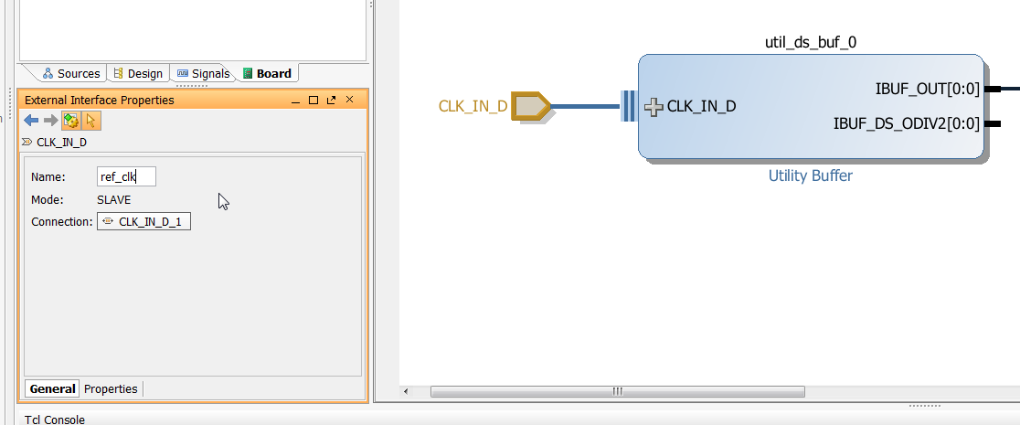
Change the name of the created external port to
ref_clk using the External Interface Properties window.
-
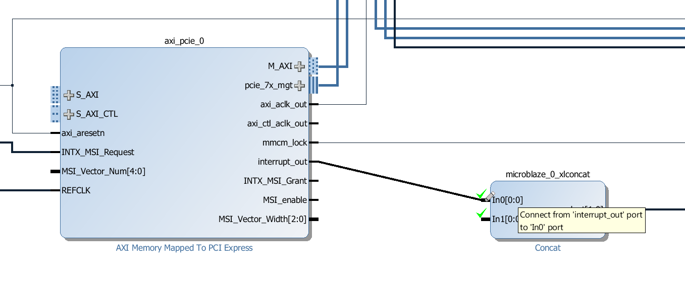
We need to connect the PCIe interrupt to the Microblaze. Connect the
interrupt_out output of the AXI-PCIe block to the “In0” input of the interrupt concat microblaze_0_xlconcat.
Add the CDMA
Now we’ll add a Central DMA to this design which will allow us to setup data transfers between the PCIe end-point and the DDR3 memory. We won’t actually test the CDMA in this tutorial series, but it’s an important part of any PCIe design that needs to transfer large amounts of data very quickly over the PCIe link. We will add an AXI Interconnect to allow the CDMA to access both the PCIe end-point and the MIG.
-
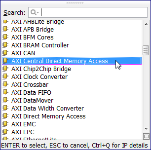
Add a “AXI Central Direct Memory Access” from the IP Catalog to the block design.

-
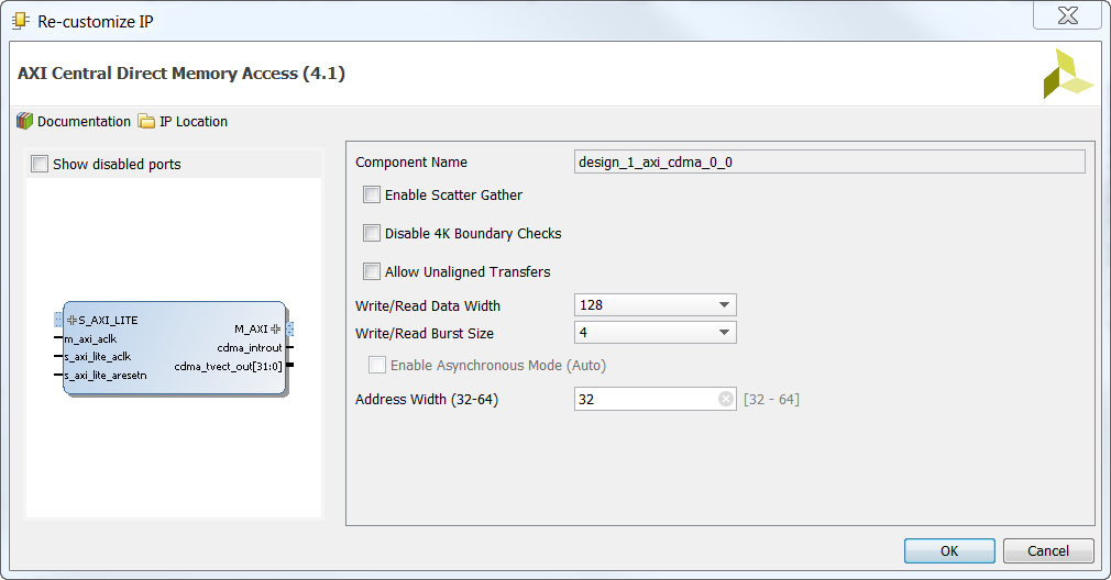
Double click on the CDMA block to open the configuration window. Disable Scatter Gather and set “Write/Read Data Width” to 128 as shown in the image below.

-
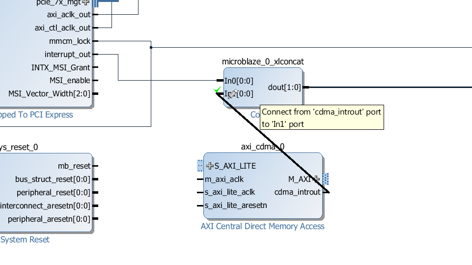
Connect the
cdma_introut output of the CDMA to the “In1” input of the interrupt concat microblaze_0_xlconcat.
-
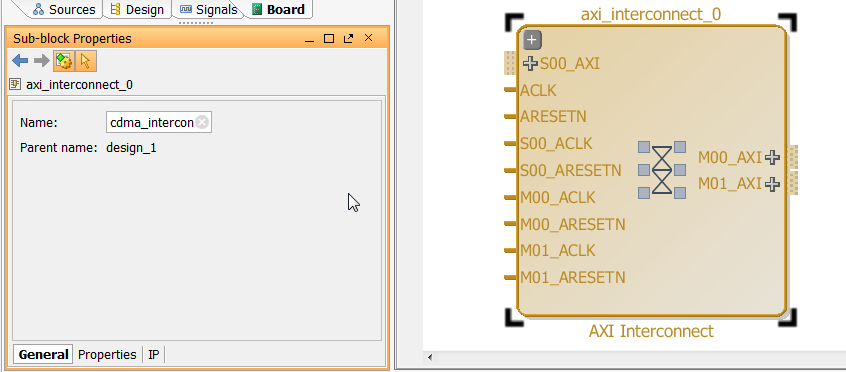
Add an “AXI Interconnect” from the IP Catalog to the block design. Rename it to
cdma_intercon using the “Sub-block Properties” window.
-
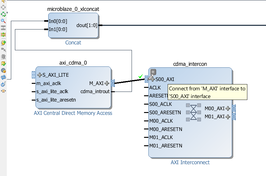
Connect the
M_AXI interface of the CDMA to the S00_AXI interface of the cdma_intercon.
-
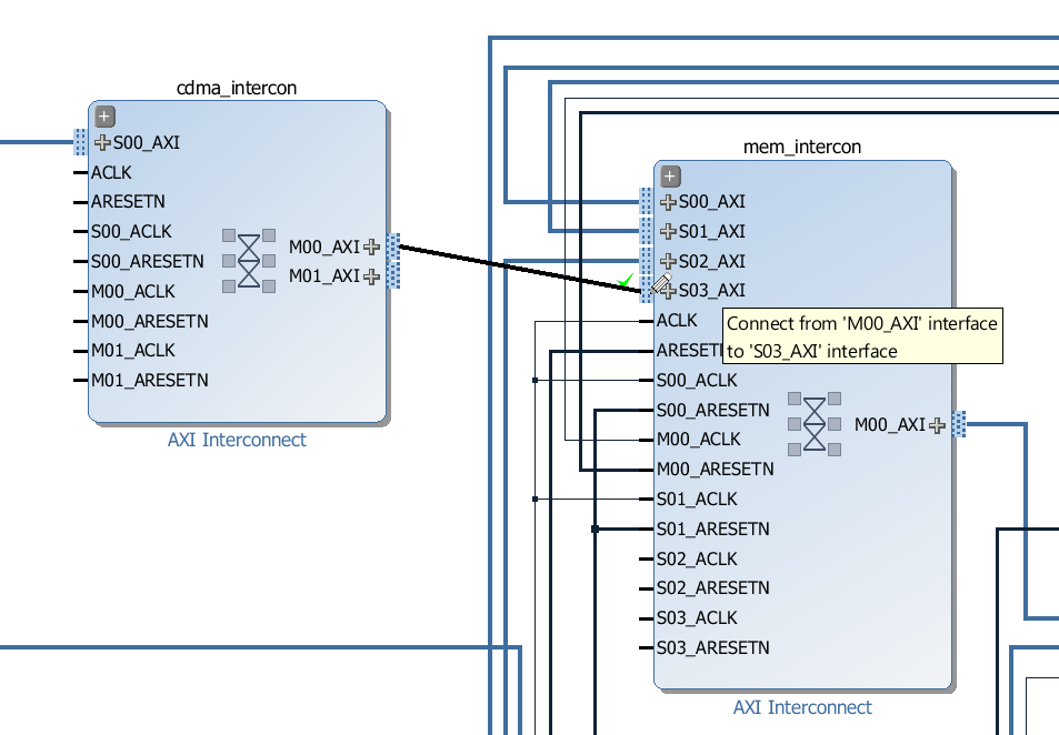
Connect the
M00_AXI interface of the cdma_intercon to the S03_AXI interface of the mem_intercon. This provides the data path between the CDMA and the DDR3 memory.
-
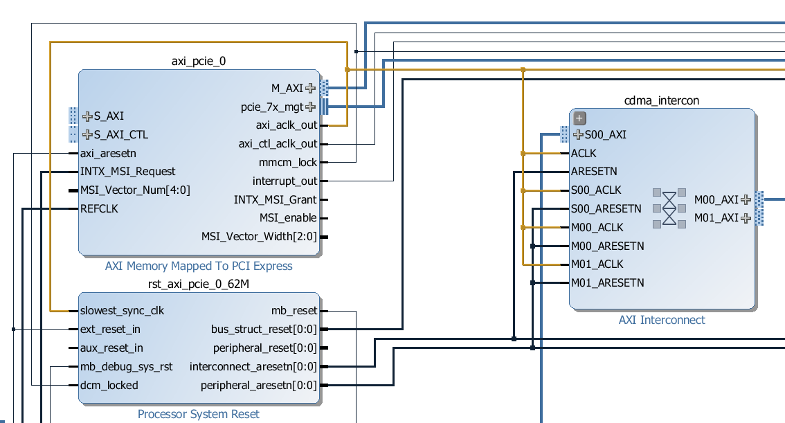
Now connect all the clocks and resets of the
cdma_intercon as shown in the image below. Connect all the clock inputs to the axi_aclk_out output of the AXI-PCIe block. Connect the “ARESETN” input to the interconnect_aresetn output of the rst_axi_pcie_0_62M Processor System Reset. Connect all other reset inputs to the peripheral_aresetn output of the rst_axi_pcie_0_62M Processor System Reset.
-
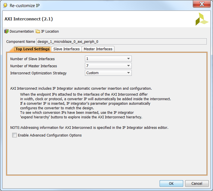
Double click on the
microblaze_0_axi_periph interconnect and configure it for 7 master ports. Leave the number of slave ports as 1.
-
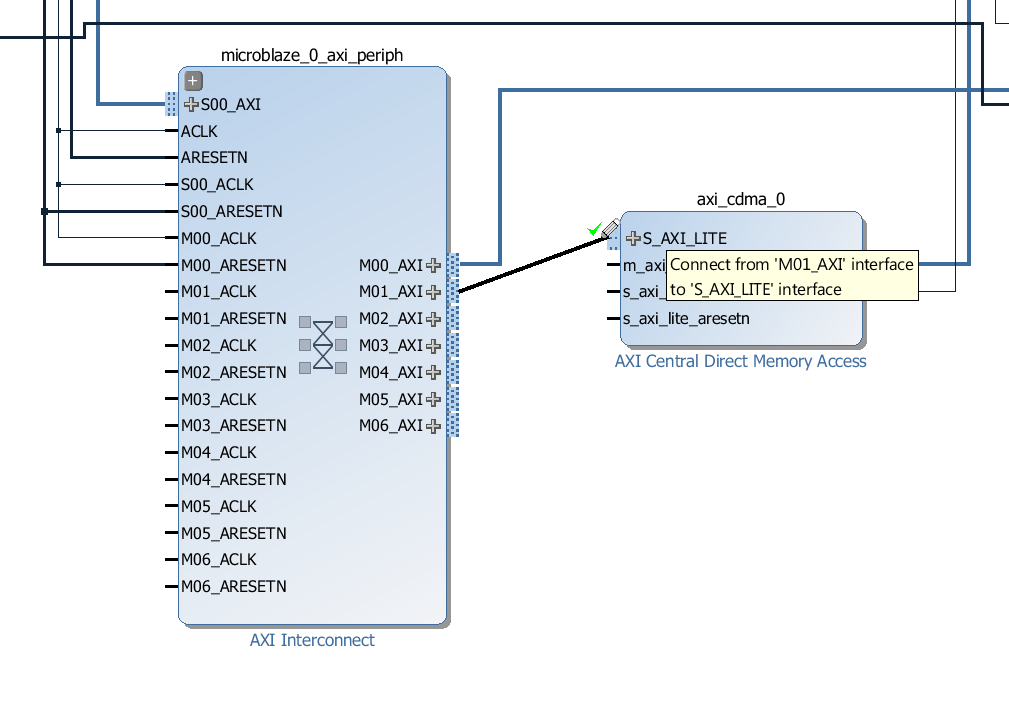
Connect the
M01_AXI interface of the microblaze_0_axi_periph interconnect to the S_AXI_LITE interface of the CDMA.
-
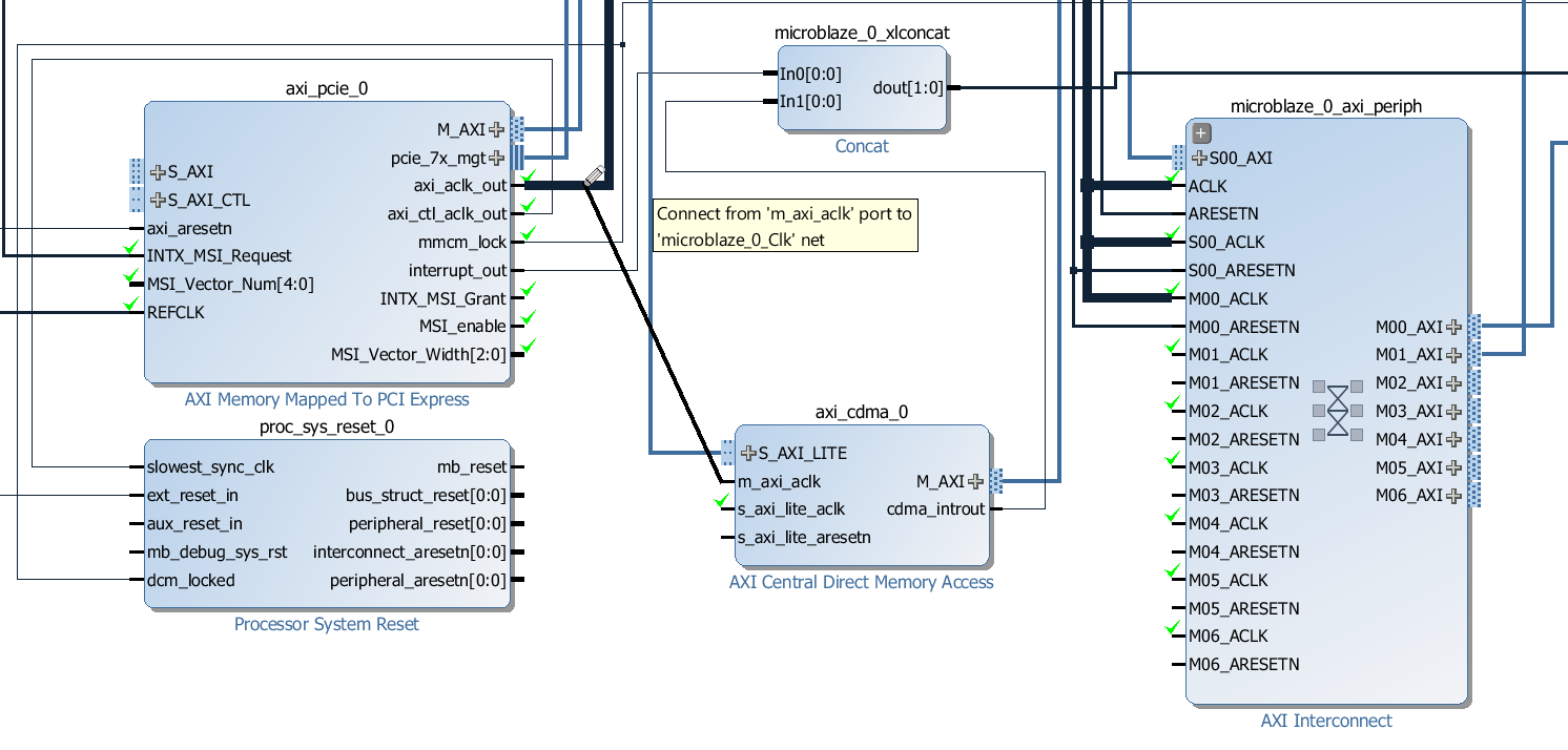
Connect the
m_axi_aclk input of the CDMA to the axi_aclk_out output of the AXI-PCIe block.
-
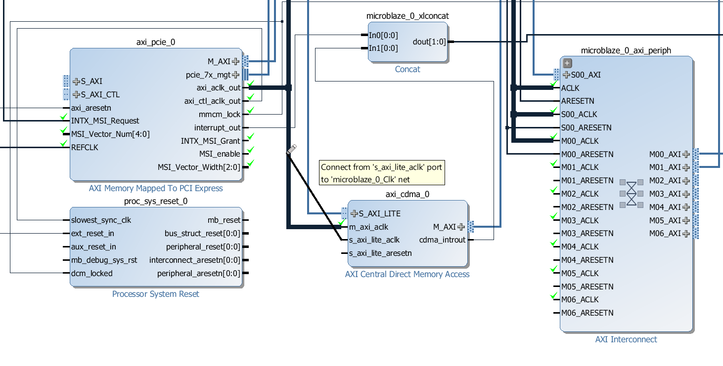
Connect the
s_axi_lite_aclk input of the CDMA to the axi_aclk_out output of the AXI-PCIe block.
-
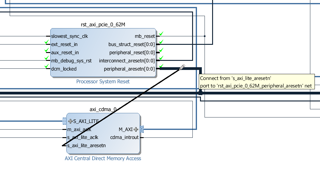
Connect the
s_axi_lite_aresetn input of the CDMA to the peripheral_aresetn output of the rst_axi_pcie_0_62M Processor System Reset block.
-
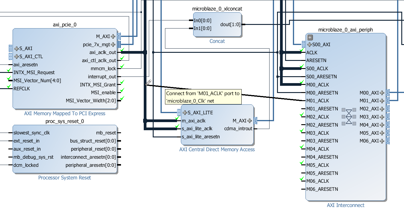
Connect the
M01_ACLK input of the microblaze_0_axi_periph to the axi_aclk_out output of the AXI-PCIe block.
-
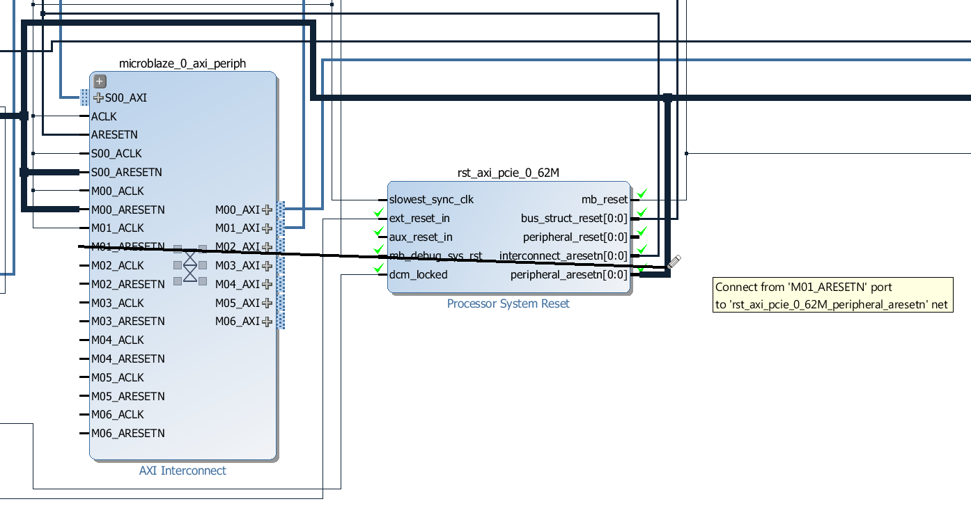
Connect the
M01_ARESETN input of the microblaze_0_axi_periph to the peripheral_aresetn output of the rst_axi_pcie_0_62M Processor System Reset block.
Connect the AXI PCIe slave interfaces
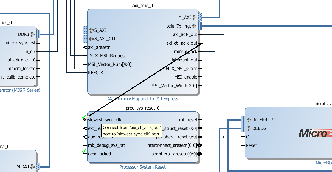
The AXI PCIe block has one slave interface for configuration (S_AXI_CTL) and another for accessing the PCIe end-point (S_AXI). The slave interface for configuration must be driven synchronous to the axi_ctl_aclk_out clock, so before connecting the slave interfaces, we first need to create a Processor System Reset to generate a reset signal that is synchronous to this clock.
-
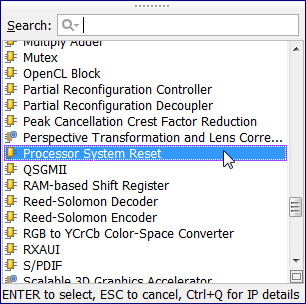
Add a “Processor System Reset” from the IP Catalog.

-
Connect the
axi_ctl_aclk_out clock output of the AXI-PCIe block to the slowest_sync_clk input of the Processor System Reset just added.
-
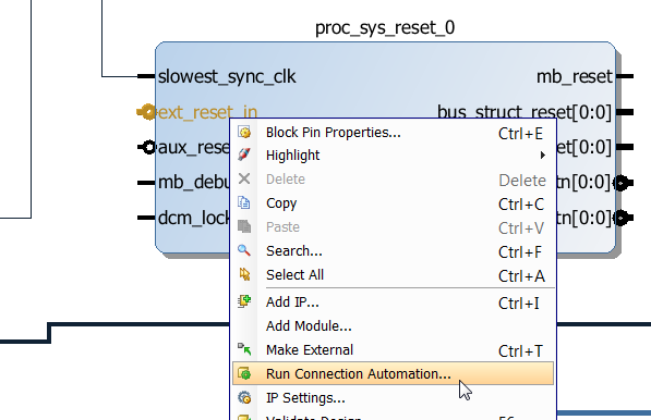
Right click on the
ext_reset_in input of the Processor System Reset and select “Run Connection Automation”, then click OK.
-
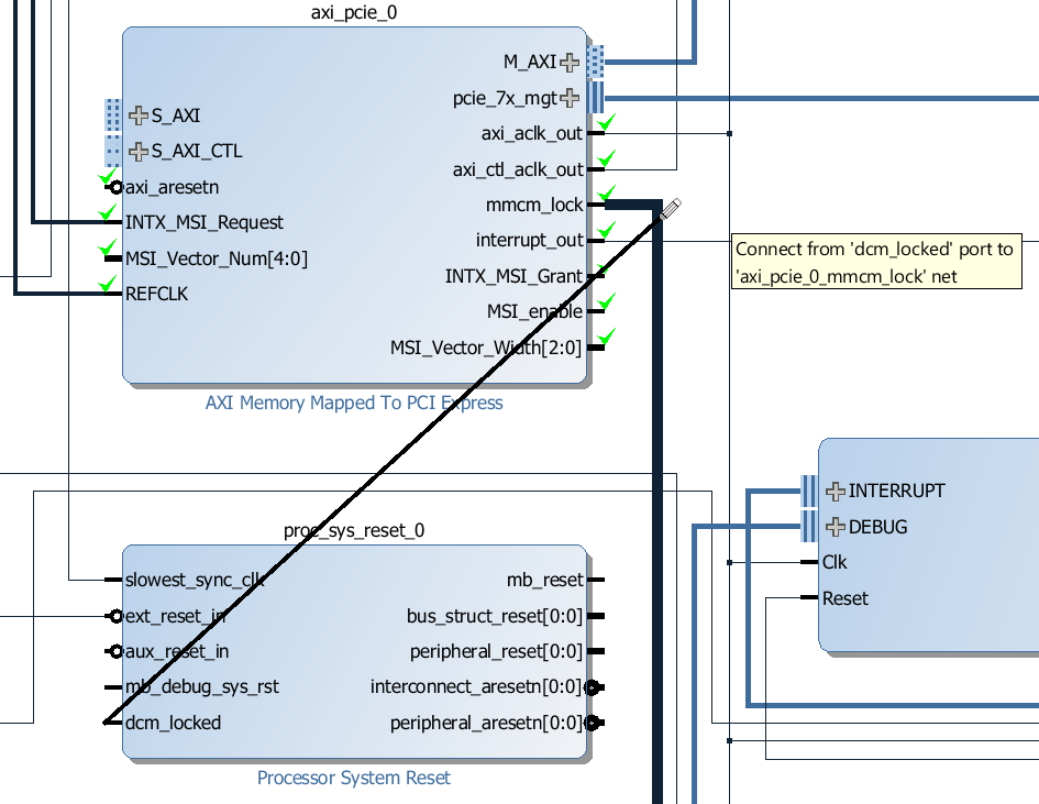
Connect the
dcm_locked input of the Processor System Reset to the mmcm_lock output of the AXI-PCIe block.
-
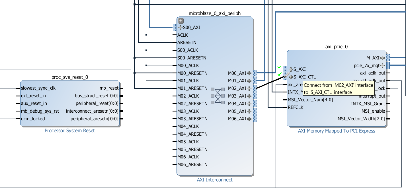
Now the Processor System Reset is setup and we can connect the AXI-PCIe block slave control interface. We want the control interface to be connected to the Microblaze, just like any other peripheral. Connect the
M02_AXI interface of the microblaze_0_axi_periph interconnect to the S_AXI_CTL interface of the AXI-PCIe block.
-
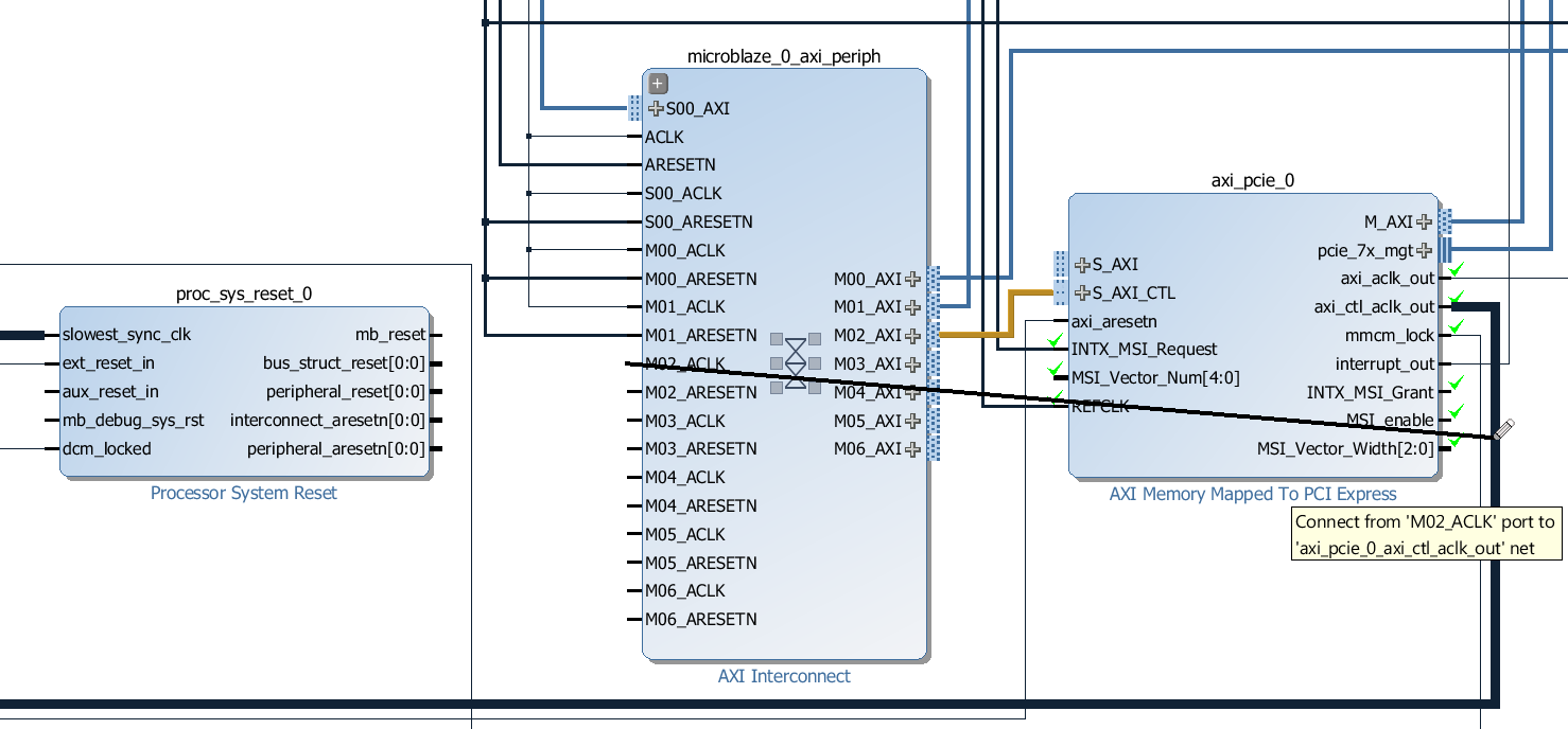
Connect the
M02_ACLK input of the microblaze_0_axi_periph interconnect to the axi_ctl_aclk_out output of the AXI-PCIe block.
-
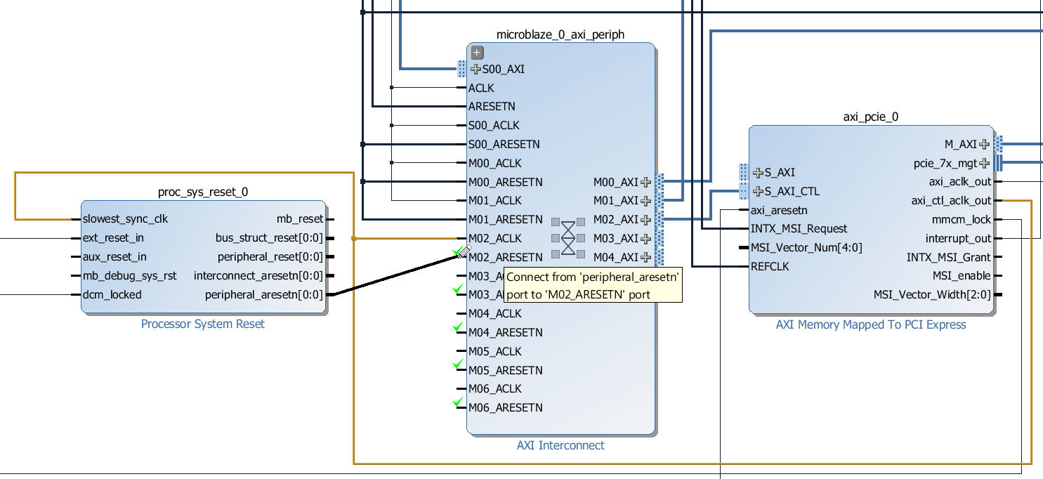
Connect the
peripheral_aresetn output of the proc_sys_reset_0 Processor System Reset to the M02_ARESETN input of the microblaze_0_axi_periph interconnect.
-
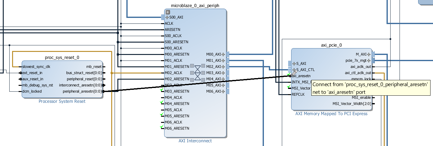
Connect the
peripheral_aresetn output of the proc_sys_reset_0 Processor System Reset to the axi_aresetn input of the axi_pcie_0 block.
-
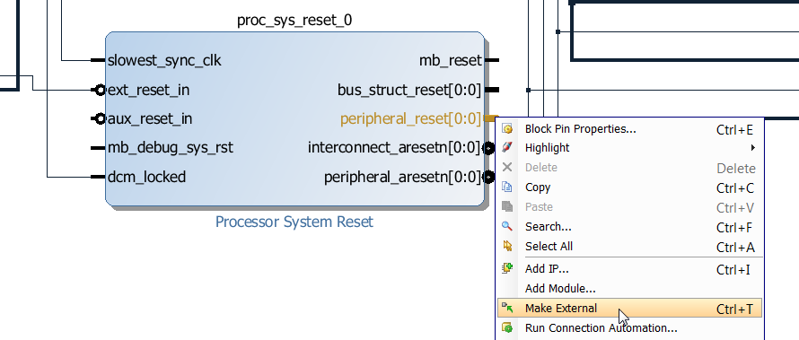
Right click on the
peripheral_reset output of the proc_sys_reset_0 Processor System Reset and click “Make External”.
-
Click on the port we just created and rename it to “perst”. This is the signal that will drive the PCIe reset input of the SSD.

The other slave interface of the AXI-PCIe block, S_AXI, provides access to the PCIe end-point address space. We want this port to be accessible to both the Microblaze and the CDMA, so we will add another AXI Interconnect to the design.
-
Add an “AXI Interconnect” from the IP Catalog to the block design. Rename it
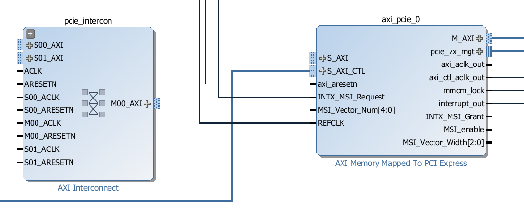
pcie_intercon and configure it to have 2 slave interfaces and 1 master interface.
-
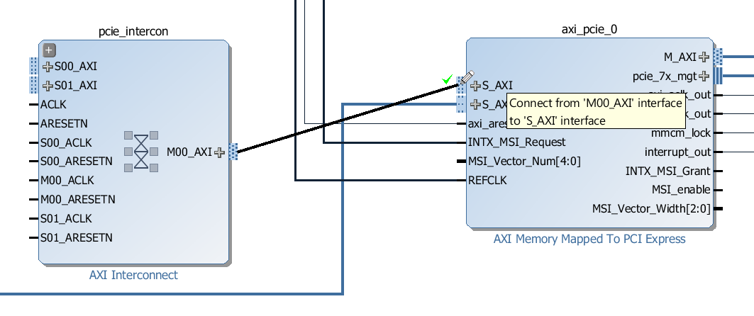
Connect the
M00_AXI interface of the pcie_intercon to the S_AXI interface of the AXI-PCIe block.
-
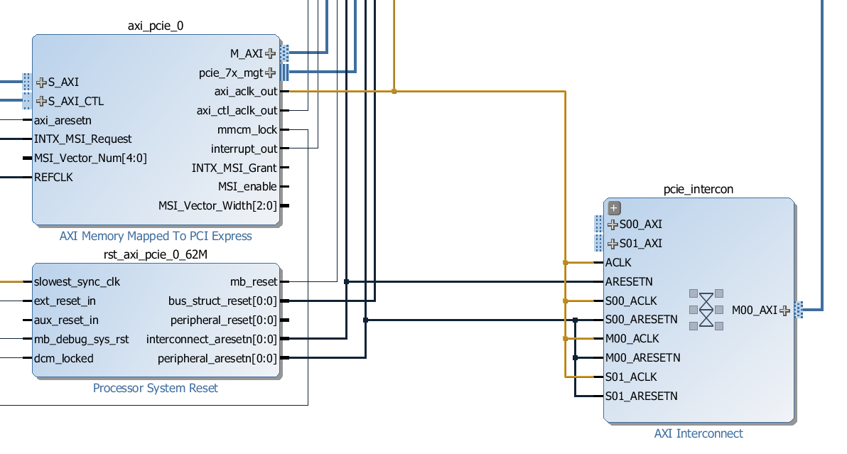
Now connect all the clocks and resets of the
pcie_intercon as shown in the image below. Connect all the clock inputs to the axi_aclk_out output of the PCIe block. Connect the “ARESETN” input to the interconnect_aresetn output of the rst_axi_pcie_0_62M Processor System Reset. Connect all other reset inputs to the peripheral_aresetn output of the rst_axi_pcie_0_62M Processor System Reset.
-
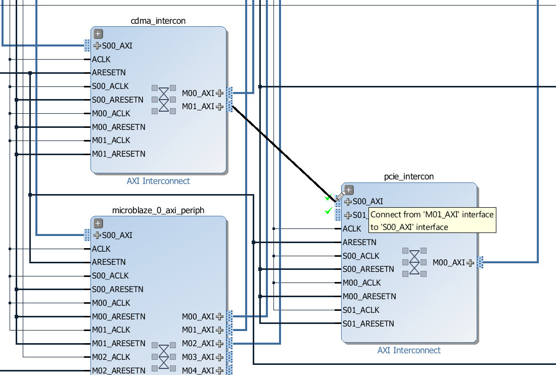
Connect the
M01_AXI interface of the cdma_intercon to the S00_AXI interface of the pcie_intercon.
-
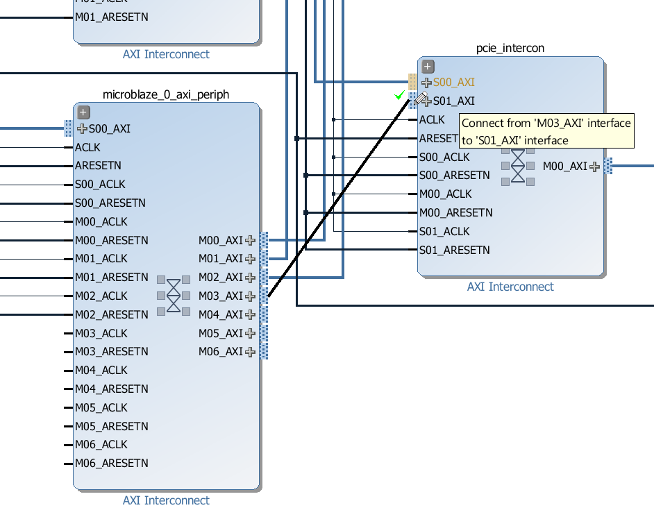
Connect the
M03_AXI interface of the microblaze_0_axi_periph interconnect to the S01_AXI interface of the pcie_intercon.
-
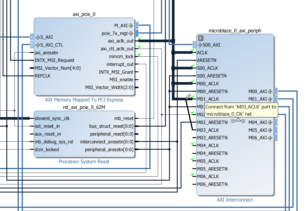
Connect the
M03_ACLK input of the microblaze_0_axi_periph interconnect to the axi_aclk_out output of the AXI-PCIe block.
-
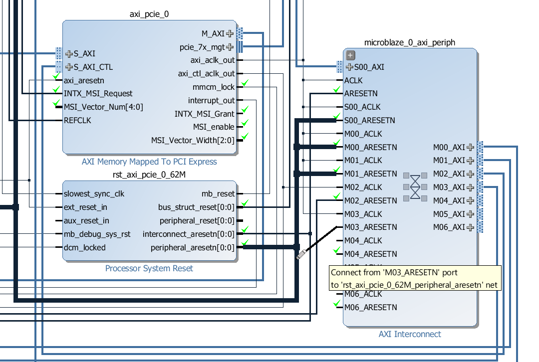
Connect the
M03_ARESETN of the microblaze_0_axi_periph interconnect to the peripheral_aresetn of the rst_axi_pcie_0_62M Processor System Reset block.
Add the other peripherals
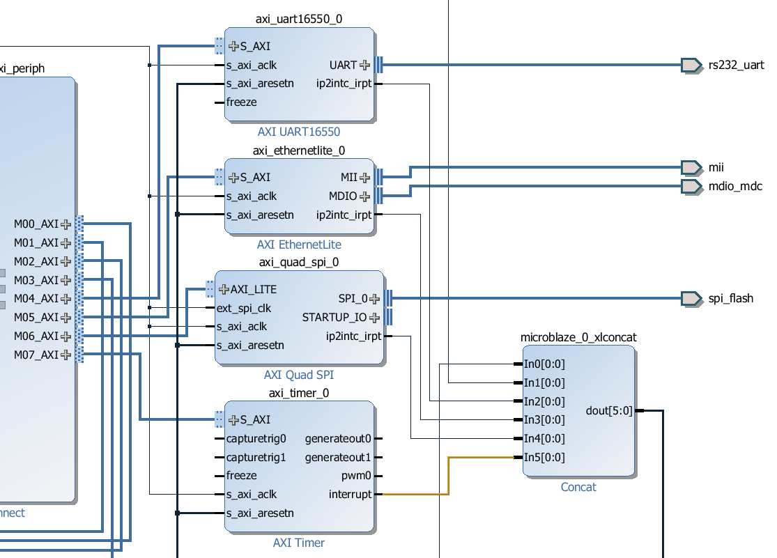
To make our design “Linux ready”, we need to add four more blocks to our design:
-
UART - for console output
-
AXI Ethernet Lite - for network connection
-
AXI Quad SPI - for retrieval of FPGA configuration files, software and Linux kernel from a QSPI Flash
-
AXI Timer - Microblaze doesn’t have an integrated timer
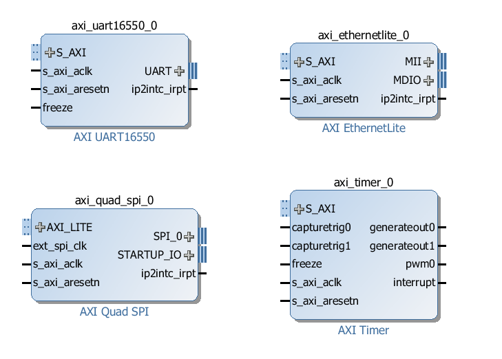
We will add all 4 blocks to the design and then let the block automation feature handle the connection of these peripherals to the Microblaze.
-
Add an “AXI UART16550” from the IP Catalog to the block design.
-
Add an “AXI EthernetLite” from the IP Catalog to the block design.
-
Add an “AXI Quad SPI” from the IP Catalog to the block design.
-
Add an “AXI Timer” from the IP Catalog to the block design.

-
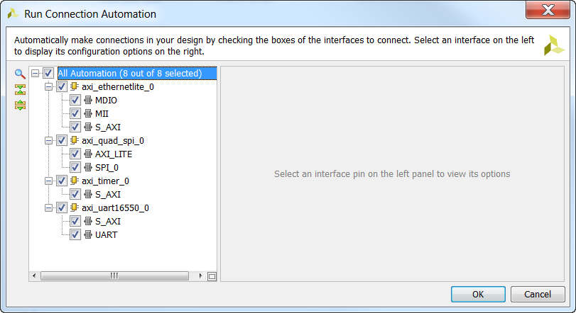
Click “Run Connection Automation” and select all of the connections for the 4 added peripherals.

-
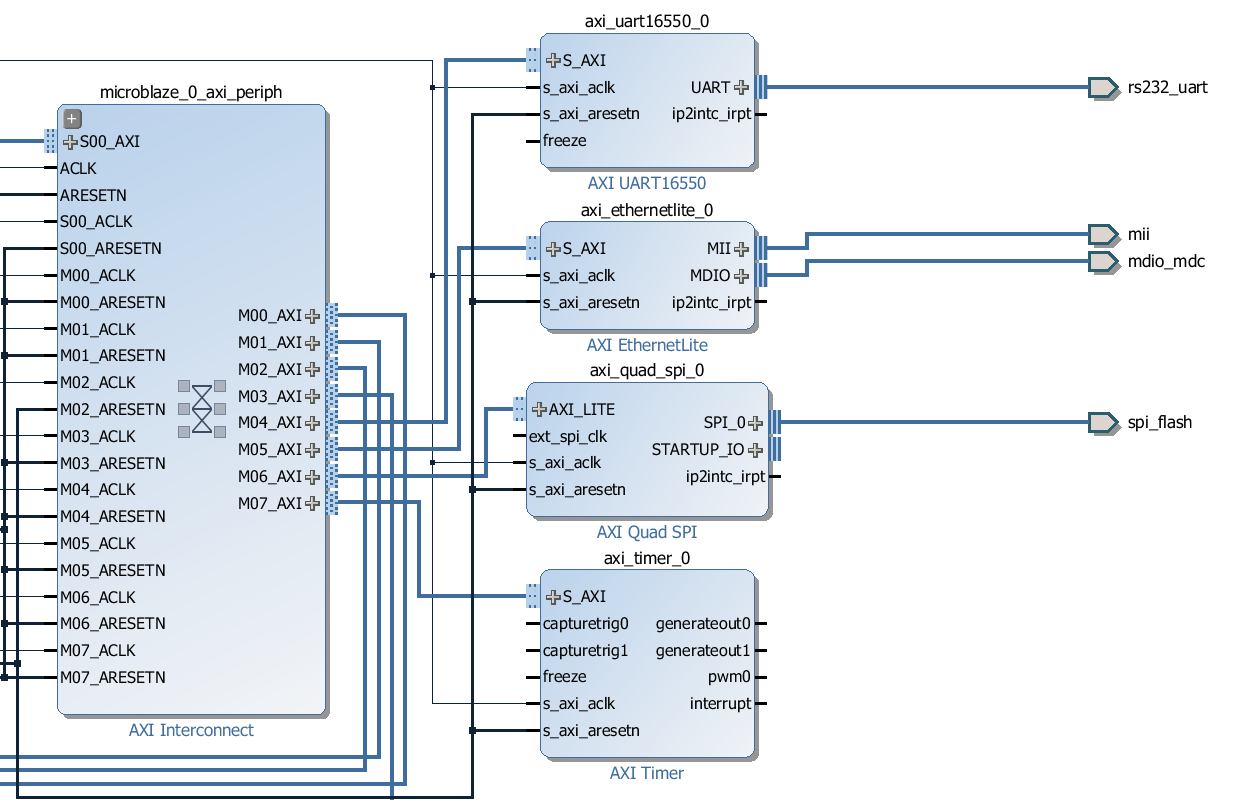
They will all have been automatically connected to the
microblaze_0_axi_periph interconnect as shown in the image below.
-
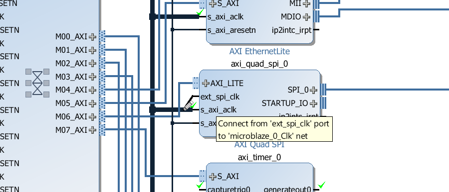
Connect the
ext_spi_clk input of the AXI QSPI to the same clock as it’s s_axi_aclk input.
-
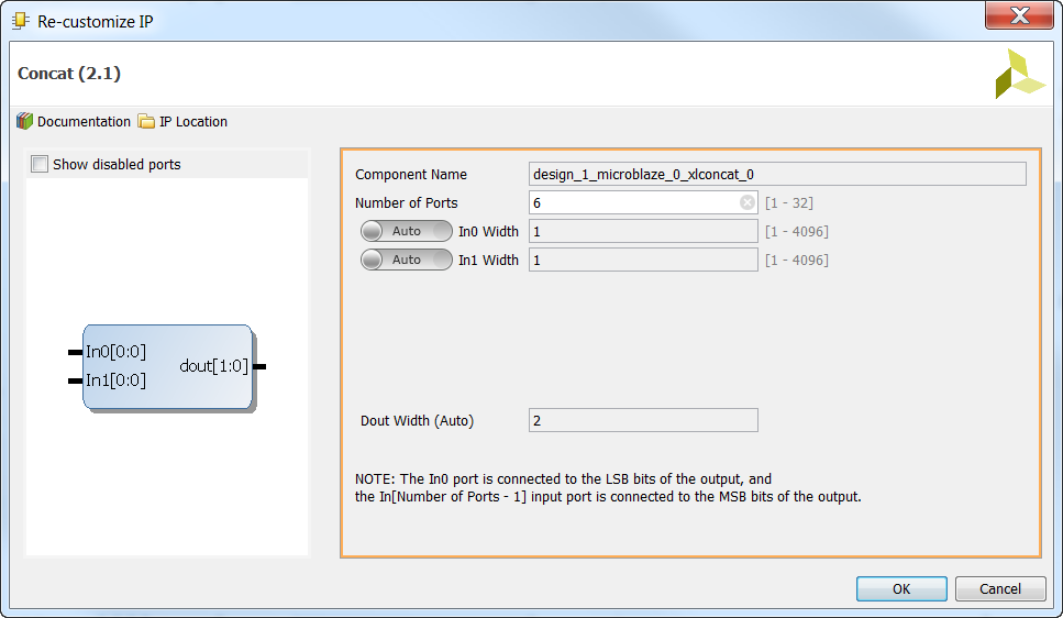
Double click on the
microblaze_0_xlconcat interrupt concat and change the number of input ports to 6 - we need 4 more to connect the interrupts of our new peripherals.
-
One-by-one, connect the interrupt outputs of the peripherals to the inputs of the interrupt concat as shown in the image below. The interrupt output for the UART, AXI EthernetLite and AXI QSPI is called
ip2intc_irpt. The interrupt output for the AXI Timer is called “interrupt”.
Add some debug signals
It’s always nice to have an LED light up to tell us that things are working correctly.
-
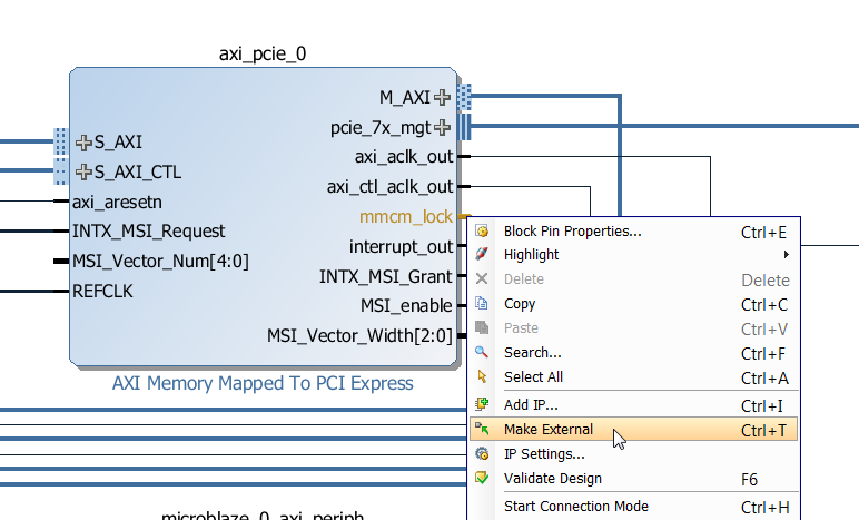
Right click on the
mmcm_lock output of the AXI-PCIe block and select “Make External”.
-
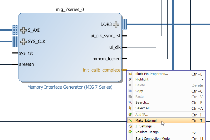
Right click on the
init_calib_complete output of the MIG and select “Make External”.
We will later add a constraint for each one of these ports to assign it to a specific LED on the KC705 board.
Assign addresses
-
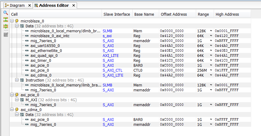
Open the “Address Editor” tab and click the “Auto Assign Address” button.

-
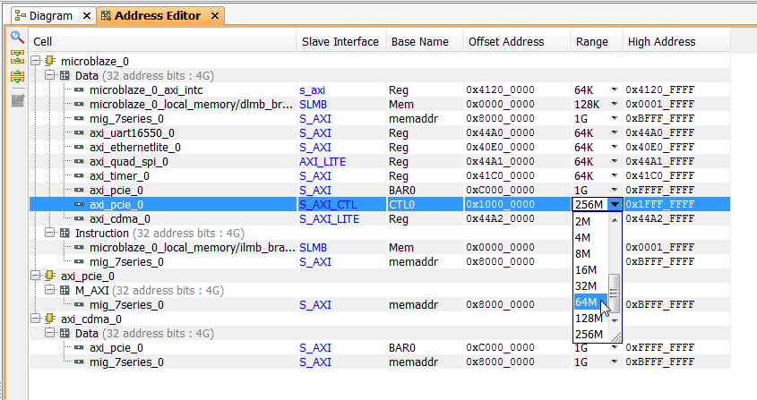
All addresses should be assigned as in the image below.

-
By default, the AXI-PCIe control interface (S_AXI_CTL) is allocated 256M, but this will cause a problem for PetaLinux later on, so change it to 64M and then save the block design.

Create the HDL wrapper
Now the block diagram is complete, so we can save it and create a HDL wrapper for it.
-
Open the “Sources” tab from the Block Design window.
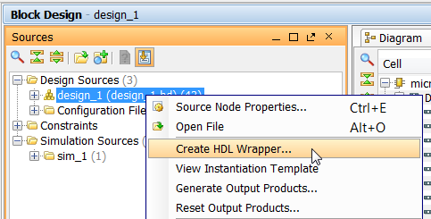
-
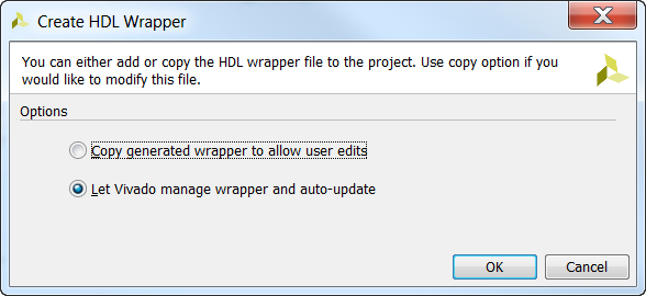
Right-click on “design_1” and select “Create HDL wrapper” from the drop-down menu.

-
From the “Create HDL wrapper” window, select “Let Vivado manage wrapper and auto-update”. Click “OK”.

Add the constraints
We must now add our constraints to the design for assignment of the PCIe integrated block, the gigabit transceivers, the reference clocks, the LEDs and a few other signals.
-
Download the constraints file from this link: Constraints for Microblaze PCIe Root Complex design
-
Save the constraints file somewhere on your hard disk.
-
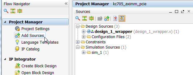
From the Project Manager, click “Add Sources”.

-
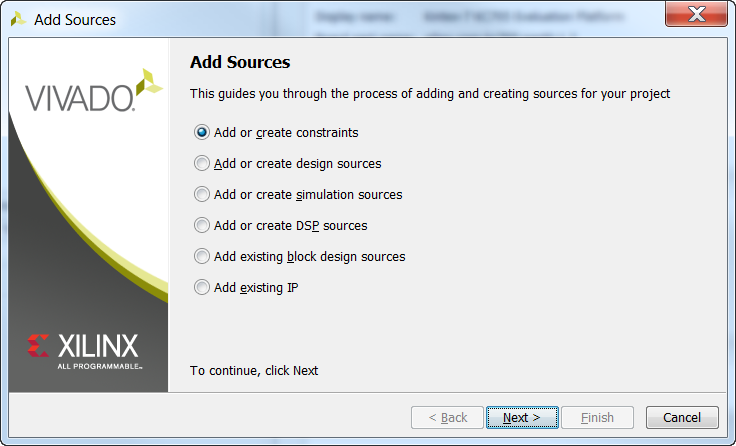
Then click “Add or create constraints”.

-
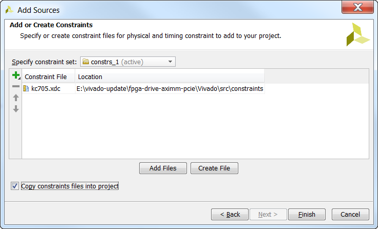
Then click “Add files” and browse to the constraints file that you downloaded earlier. Select the constraints file, then click “OK”. Now tick “Copy constraints files into project” and click “Finish”.

-
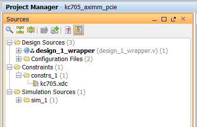
You should now see the constraints file in the Sources window.

Finished at last!
In the next tutorial: Zynq
In the next part of this tutorial series, we will build another PCIe Root Complex design in Vivado, but this time for the Zynq. The target hardware will be the PicoZed 7Z030 and the PicoZed FMC Carrier Card V2.
Testing the project on hardware
In the third and final part of this tutorial series, we will run a stand-alone application on the hardware which will check the state of the PCIe link and enumerate the connected PCIe end-points. Then we will run PetaLinux on our hardware and make an NVMe PCIe SSD accessible under the operating system.
Sources Git repository
The sources for re-generating this project automatically can be found on Github here: FPGA Drive PCIe Root Complex design
Other useful resources
Here are some other useful resources for creating PCI Express designs:
If you have any questions about this tutorial, or if you run into problems, please leave me a comment below.

